EP-Scan for SI Applications
Demos
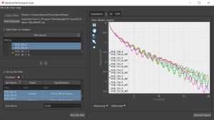
Explore how EP-Scan enables early signal integrity analysis within PCB layout workflows, allowing channel behavior to be evaluated and potential risks identified before final verification.
By the end of this session, PCB designers can:
- Import ODB++ and IPC 2581 layout designs
- Review and refine stack-up definitions
- Analyze insertion loss, return loss, and TDR response
- Compare channel behavior across multiple nets
- Generate eye diagrams based on channel performance
- Identify layout concerns such as via stubs and return path discontinuities