


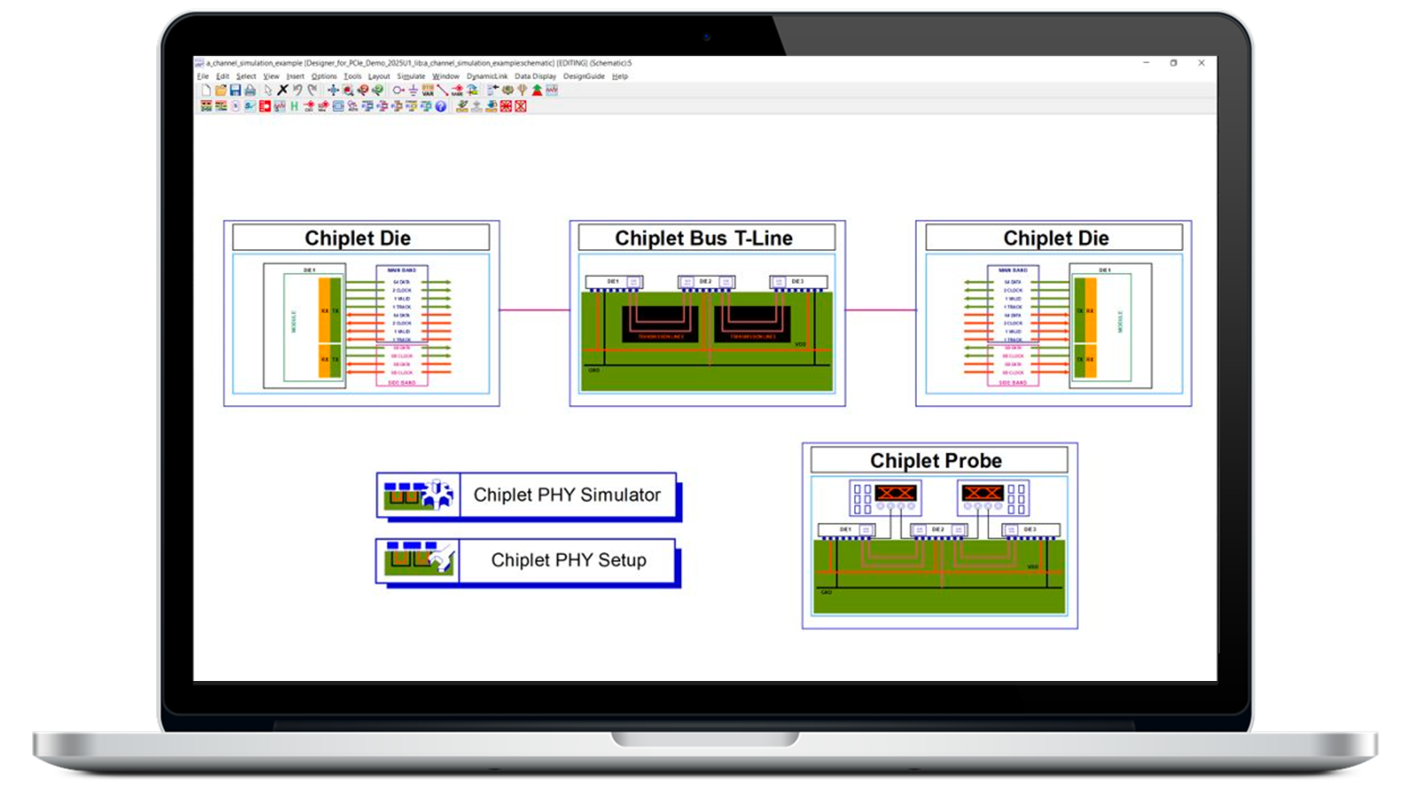
Why Use Chiplet PHY Designer
Design, validate, and optimize chiplet-based systems from architecture through package implementation.
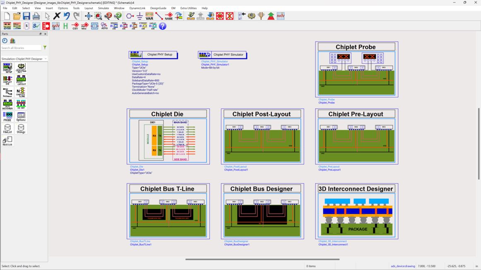
Chiplet-based systems are emerging as the new scaling paradigm, moving beyond the limitations of monolithic SoC design. As process scaling becomes increasingly difficult and costly, system complexity is shifting from “within a die” to “across multiple dies”. This transition is enabled by advanced heterogeneous integration technologies such as 2.5D/3DIC packaging, silicon interposers, and bridge-based architectures like EMIB, together with standardized die-to-die connectivity such as UCIe. Chiplet PHY Designer supports chiplet-based design workflows, enabling faster and more reliable end-to-end chiplet-based system development. It supports the latest industry standards, including UCIe 3.0 and BoW 2.0, along with compliance-driven metrics such as VTF-based validation, helping ensure robust die-to-die link performance early in the design cycle.
Key Capabilities

Evaluate heterogeneous integration design alternatives.

Optimize multi-die package performance and reliability.

Validate die-to-die communication and interfaces.

Improve power, scalability, and efficiency targets.

Reduce integration risks before hardware fabrication.

Improve manutacturing readiness and product quality.
Resources to Get You Started
Chiplets are a promising alternative to monolithic SoCs, offering lower costs, higher performance, and greater flexibility. Chiplets are also a key enabler of heterogeneous and modular SoC design, which can accelerate innovation and adaptation in the electronic industry. However, it’s essential to acknowledge the trade-offs inherent in this transition. The increased design complexity, particularly in probing and D2D communication, emphasizes the importance of having the right tools in the design workflow.

Bootcamps
Designing with Chiplets and Advanced Packaging to build system-on-chips (SoCs)

blogs
What is a Chiplet, and Why Should You Care?

Technical Overviews
Keysight EDA Electronic Design Automation Software

Demos
Chiplet System Analysis Challenges and Solutions
Lessons
Fast Track Chiplet Integration with Streamlined UCIe's Electrical Layer Analysis

Lessons
UCIe vs BoW: Your Essential Guide to Choosing the Right Chiplet Standard
Application Notes
How to Detect Signal Integrity Issues in Chiplet Designs Early
Have Questions? We've Got Answers
Chiplets are smaller functional dies that can be combined into a single package to create complex systems. They improve design flexibility, scalability, performance optimization, and development efficiency compared to monolithic SoCs.
Chiplet-based systems introduce challenges related to package design, die-to-die communication, verification, interoperability, testing, thermal management, and manufacturing complexity.
EDA software enables design exploration, simulation, optimization, verification, validation, characterization, and test planning to help engineers identify issues before fabrication and deployment.
Yes. Modern chiplet development workflows can support industry standards such as UCIe and other die-to-die interconnect technologies to promote interoperability and ecosystem growth.
Organizations can reduce development costs, accelerate innovation, improve scalability, optimize system performance, leverage heterogeneous integration, and shorten time-to-market for advanced semiconductor products.