Co-Packaged Optics (CPO) Design Solutions
Connect photonic device, PIC, electronic, packaging, and system-level design decisions for emerging optical I/O architectures.




Key Design Challenges in Co-Packaged Optics
Evaluate the optical, electrical, packaging, and system tradeoffs that determine CPO performance.
Bringing the optical engine closer to the switching or compute silicon shortens the high-speed electrical path, but it also connects the optical, electrical, packaging, thermal, and system domains more closely. Changes in one domain can affect performance across the others, making system-level evaluation essential.
In CPO, the photonic device, PIC, optical link, package, electronics, and system can no longer be evaluated as isolated domains.

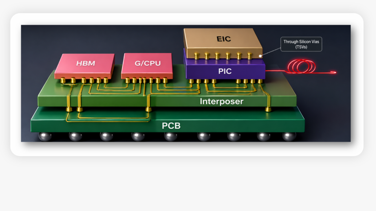
Address CPO Challenges Across the Design Flow
Move seamlessly from photonic device design to optical coupling, PIC development, and system validation.
- System
- PIC Co-Design
- Optical I/O
- Packaging
- Devices
Assess Link and Architecture Performance
Use system and circuit simulation to investigate how photonic and electronic behavior affects the performance of optical links and transceiver architectures.
- Electro-optical-electrical link behavior
- Transmitter and receiver interactions
- Wavelength-division multiplexing architectures
- Component impairments and nonlinear behavior represented in system models
- Design tradeoffs before hardware integration

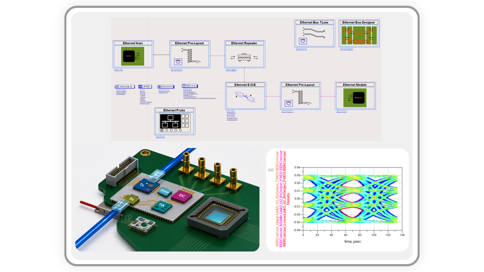
Connect Device, Circuit, and Layout
Combine RSoft device simulation with ADS Photonic Designer to create and refine photonic building blocks, design PIC circuits and layouts, and evaluate electro-optical-electrical behavior.
- Create and optimize custom photonic devices
- Use device results in PIC and electro-optical circuit simulations
- Develop schematic and layout-based PIC designs
- Work with foundry PDKs and model formats
- Evaluate how component behavior affects circuit and system response


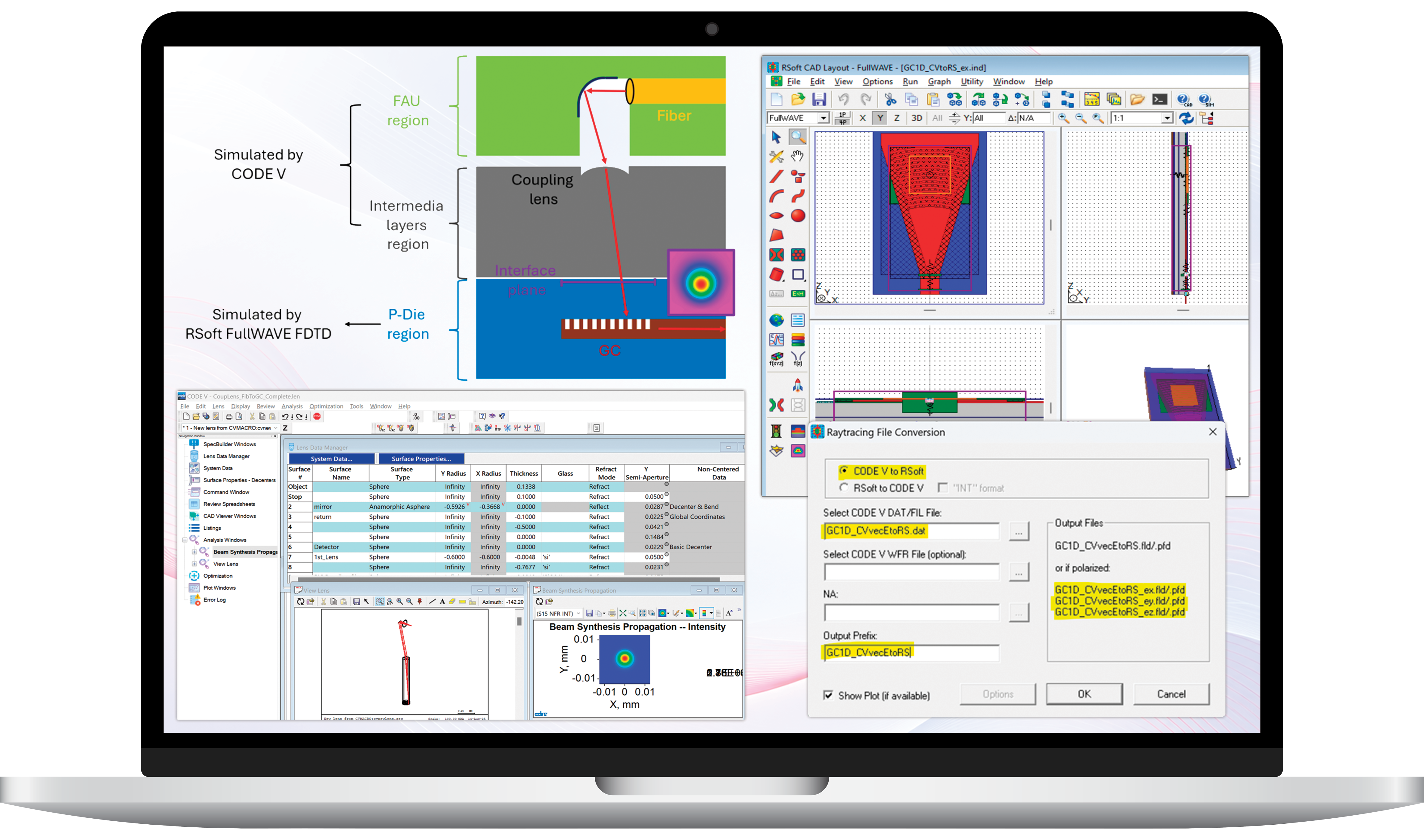
Evaluate Fiber-to-PIC Coupling
CPO architectures depend on efficient coupling between fibers, coupling optics, and on-chip photonic structures. Keysight tools can analyze important parts of this optical path:
- Use CODE V to design and analyze coupling optics and larger free-space propagation regions.
- Use RSoft to simulate fiber-to-chip interfaces, waveguides, grating couplers, edge couplers, and other photonic structures.
- Evaluate coupling efficiency, alignment sensitivity, and tolerances within the appropriate tool and model.

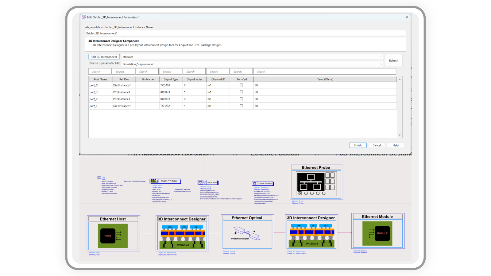
Analyze High-Speed Package Interconnects
Use Keysight electronic design and electromagnetic analysis tools to evaluate package and interconnect structures that influence CPO performance.
- Package interconnects, vias, bumps, and substrate structures
- High-speed channel behavior
- Signal integrity and power integrity considerations
- Electrical and packaging tradeoffs that affect the integrated architecture

Design Critical Photonic Components
Use RSoft Photonic Device Tools to model and optimize photonic structures used in optical interconnects and PICs.
- Grating and edge couplers
- Spot-size converters and inverse tapers
- Silicon photonic waveguides and compact bends
- Modulators and photodetector structures
- Photonic crystal, metasurface, and metalens structures
Available methods include FDTD, BPM, FEM, EME, RCWA, topology optimization, inverse design, and multi-parameter optimization, depending on the device and physics required.


Optimize Your CPO Design Workflow
Apply topology optimization, inverse design, parameter scanning, distributed computing, and GPU acceleration to improve structures such as couplers, compact bends, and wavelength-selective devices. Keysight optical and electronic design experts can also help define a practical workflow for photonic components, PIC circuits, package interconnects, optical alignment, and system evaluation.
- Photonic component simulation and optimization
- PIC design and electro-optical circuit simulation
- Package and high-speed interconnect analysis
- Optical coupling and alignment studies
- System architecture and link evaluation
- Custom workflow and model development
Accelerate Development with Optical Design Experts
Whether you're evaluating new optical interconnect architectures or optimizing an existing PIC platform, Keysight's optical engineering experts can help with:
- Optical coupling design
- PIC optimization
- Fiber alignment analysis
- System architecture evaluation
- Simulation workflow development
- Custom photonic modeling services


Discover CPO Resources
Application Notes
Grating Assisted Coupler

Application Notes
Subwavelength Grating Structure
Application Notes
Custom PDK Generation for a Ring Resonator
Application Notes
Electro-Absorption Modulator
Application Notes
Simulation of Long-Period Fiber Gratings Formed with Helical Fiber