


- Overview
- All Models
- Support
Reliable in-circuit defect detection for PCB manufacturing
Keysight in-circuit test systems provide high-performance, scalable solutions for testing complex, densely populated printed circuit boards in high-volume manufacturing. With flexible pin configurations, boundary scan support, vectorless test capabilities, and programmable analog measurements, these systems ensure fast and accurate detection of assembly faults such as solder defects, misoriented components, and wrong values. Built-in diagnostics, intuitive test development tools, and automation-ready integration streamline production workflows while reducing false calls and improving first-pass yield. Request a quote for one of our popular configurations today. Need help selecting? Check out the resources below.
High fault coverage
Detects a wide range of structural defects, such as solder opens, shorts, and incorrect component placement, ensuring improved product quality and reduced rework costs.
Scalable test pin design
Supports high-density boards with flexible pin-count configurations, allowing adaptation to various board sizes and complexities without changing hardware.
Vectorless test capability
Uses capacitive sensing to detect device presence and orientation without requiring a powered-up unit under test, which is ideal for testing complex digital assemblies safely.
Integrated boundary scan
Performs structural diagnostics through standard test access ports (TAPs), eliminating the need for intrusive probing or additional hardware instrumentation.
-
System width
800 mm to 1800 mm
-
Maximum node count
0 to 5760
-
Maximum parallel testing
2 to 112
-
Fixture actuation
Vacuum, Press down
Most popular configurations
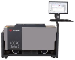
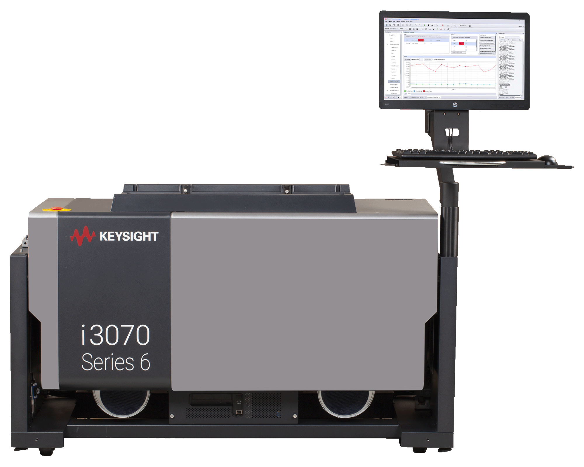
4-Module ICT System, i307x Series 6
2-Module ICT System, i317x Series 6

In-Line 2-Module ICT System; i337x, Series 5i
Services and support
Innovate at speed with curated support plans and prioritized response and turn-around times.
Get predictable, lease-based subscriptions and full lifecycle management solutions—so you reach your business goals faster.
Experience elevated service as a KeysightCare subscriber to get committed technical response and more.
Ensure your test system performs to specification and meets local and global standards.
Make measurements quickly with in-house, instructor-led training, and eLearning.
Download Keysight software or update your software to the newest version.
Frequently asked questions
An in-circuit test system (ICT) is a diagnostic tool used to verify the integrity and correct assembly of individual components on a printed circuit board (PCB) after the manufacturing process. Unlike functional testing, which validates the overall behavior of a complete device, ICT focuses on checking each component independently, such as resistors, capacitors, diodes, transistors, and ICs for correct value, orientation, placement, and electrical performance.
ICT systems use a bed-of-nails fixture to contact specific PCB test points. This allows the system to measure voltage, current, resistance, and other electrical parameters for each component. The main advantage of ICT is early fault detection in the production line, which reduces rework and repair costs. It can catch common assembly errors like missing components, wrong values, solder bridges, and open connections. ICT is ideal for high-volume manufacturing due to its fast test time and high fault coverage, especially for boards with high component density.
An in-circuit test system detects manufacturing defects by applying electrical signals to specific test nodes on a PCB and analyzing the response. The system uses a network of test probes or pins to access these nodes, which connect to the component leads or designated test points. It then performs measurements, such as resistance, capacitance, diode voltage drops, or transistor gain to determine whether each component is installed correctly and within tolerance.
Shorts and opens are detected using continuity tests that apply a voltage and measure resulting currents between nets that should or should not be connected. Misoriented or misplaced components are found by comparing the measured behavior against known good values. For example, a reversed diode will fail the forward voltage test. Some systems also support powered-up testing of digital components or limited boundary scan access for devices with Joint Test Action Group (JTAG) support.
The goal is to find defects early in the production process, enabling rapid correction and reducing the cost and time associated with downstream failure analysis and repair.
In-circuit testing offers multiple advantages that improve quality assurance and production efficiency. First, it provides high fault coverage, often detecting over 90% of manufacturing defects, including component misplacements, soldering faults, shorts, and opens. This level of detail allows manufacturers to isolate and address problems quickly, reducing repair costs and improving yield.
Second, ICT systems offer fast test cycle times, often testing a complete board in under a minute. This speed is ideal for high-volume production lines where throughput is essential. Test results are consistent and objective, reducing human error during manual inspection.
Another significant benefit is data collection and traceability. ICT systems can log test results for every board, helping manufacturers identify trends, detect process drift, and implement corrective actions based on real-time metrics. They also enable early failure detection, preventing faulty units from reaching final test or the customer, thereby reducing warranty claims and field returns.
In-circuit testing is especially beneficial for medium- to high-volume printed circuit board assemblies (PCBAs) with moderate to high component counts. It is well-suited for boards that include a mix of analog and digital components, passive devices, and integrated circuits. Manufacturing environments with automated surface-mount technology (SMT) and through-hole processes also benefit, as ICT systems can verify both components.
Assemblies that are used in automotive, consumer electronics, medical devices, industrial controllers, and telecommunications equipment commonly undergo ICT. These applications require high quality and reliability, and early detection of assembly issues is critical. PCBs that have complex routing and high-density packaging benefit even more, as visual inspection becomes impractical.
In-circuit testing is less effective for low-volume or highly complex boards with limited test access. Functional testing, boundary scan, or flying probe testing may be more suitable in those cases. However, ICT remains a cornerstone for ensuring assembly quality for mainstream electronics manufacturing.
Creating a test program for an in-circuit test system involves several key steps. First, test engineers import design data—such as the netlist, BOM (bill of materials), and component layout—into a software environment that supports automated program generation. This process maps each component to specific test types (resistor, capacitor, diode, IC, etc.) and assigns the corresponding test parameters.
Once the initial test plan is generated, the program is validated using a known-good board (often called a "golden board"). The system compares the actual measurements against expected values to fine-tune tolerances and eliminate false failures. Engineers may also use debugging tools to step through individual tests, modify limits, and suppress redundant or non-critical tests that may slow down the process.
After validation, the program is integrated into the production test sequence. Over time, production and failure analysis feedback can further refine the test program. Updates are easy to deploy, and automated test coverage analysis helps ensure continuous quality improvement.