


-
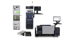
Parallel Test Systems
Scalable and flexible testing for complex board assemblies


-
Boundary Scan Analyzers
Efficient fault isolation with pin-level precision

-
Functional Test Systems
Integrated functional test system for reliable production results
-
In-Circuit Test Systems
Precision fault detection for high-density boards

Parallel Test Systems
Keysight Parallel Test Systems provide versatile and scalable solutions for diverse manufacturing test requirements. The Advanced model offers a compact, cost-effective platform for mixed-signal PCB testing with built-in analog, digital, and boundary scan capabilities. It simplifies test development and integration, making it well-suited for lean production environments. The Expert model delivers unmatched throughput for demanding applications with thousands of simultaneous test channels, modular architecture, and comprehensive coverage, including in-circuit, boundary scan, and functional tests. This system excels in high-mix and high-volume manufacturing, providing fast diagnostics and seamless automation integration. Explore our wide range of parallel test systems from advanced to expert performance levels to find the one that is right for your application. Need help selecting? Check out the resources below.


Advanced

Expert
Boundary Scan Analyzers
Keysight boundary scan analyzers deliver advanced digital test capabilities for high-density boards, enabling precise fault isolation without requiring physical probe access. The system is designed for efficient structural testing and provides fast diagnostics of interconnects, shorts, opens, and stuck-at faults across complex digital assemblies. With seamless integration into in-circuit and functional test systems, boundary scan supports JTAG-based scan chains. It enables access to hard-to-reach nets, reducing test development time and improving coverage. Explore our boundary scan to find the one that is right for your application. Need help selecting? Check out the resources below.

Functional Test Systems
Keysight functional test systems offer a modular, flexible solution for testing complex electronic assemblies. With precision measurement, high-density switching, configurable power delivery, and synchronized signal acquisition, the system supports a wide range of analog, digital, and mixed-signal applications. Built-in automation and real-time monitoring streamline test development and improve coverage, making it ideal for validating devices like automotive ECUs, industrial controllers, and embedded boards. Explore our wide range of functional test systems to find the one that is right for your application. Need help selecting? Check out the resources below.

In-Circuit Test Systems
Keysight in-circuit test systems provide high-performance, scalable solutions for testing complex, densely populated printed circuit boards in high-volume manufacturing. With flexible pin configurations, boundary scan support, vectorless test capabilities, and programmable analog measurements, these systems ensure fast and accurate detection of assembly faults such as solder defects, misoriented components, and wrong values. Built-in diagnostics, intuitive test development tools, and automation-ready integration streamline production workflows while reducing false calls and improving first-pass yield. Explore our wide range of in-circuit test systems to find the one that is right for your application. Need help selecting? Check out the resources below.

Driving confidence in automotive electronic testing
Automotive electronics require precise and comprehensive testing to ensure reliability and safety. Keysight in-circuit test systems offer key features like low-current measurements, supercapacitor testing, LED diagnostics, and fast shorts detection, which are ideal for modules such as ECUs, engine controllers, and sensor boards. High-throughput solutions efficiently test compact boards in parallel, while boundary scan tools enhance coverage for inaccessible nodes. Together, these tools ensure performance and quality across high- and low-complexity automotive electronics.
Explore compatible software and accessories for your in-circuit test for manufacturing solution
Choose from a wide range of in-circuit test software for streamlined test program generation, advanced fault diagnosis, and enhanced test coverage. Complement your ICT system with accessories such as fixture kits, probe modules, boundary-scan tools, cable assemblies, sensor plate, single probe, and more.
Explore in-circuit test for manufacturing use cases
In-circuit test for manufacturing support a wide range of testing across various industries, discover them all.
Manufacturing
How to Perform Low-Current Measurements on PCBAs
Integrate a source measure unit into the in-circuit tester.

Manufacturing
How to Integrate an In-Circuit Tester Into Industry 4.0
In-circuit tester and IPC-CFX enable Industry 4.0 factories.
Manufacturing
How to Speed Up Short Testing for High-Impedance Nodes
Implement the enhanced short test algorithm in an in-circuit test system to improve test time for short tests.

Services and support
Innovate at speed with curated support plans and prioritized response and turn-around times.
Get predictable, lease-based subscriptions and full lifecycle management solutions—so you reach your business goals faster.
Experience elevated service as a KeysightCare subscriber to get committed technical response and more.
Ensure your test system performs to specification and meets local and global standards.
Make measurements quickly with in-house, instructor-led training, and eLearning.
Download Keysight software or update your software to the newest version.
Frequently asked questions
In-Choose an ICT system based on PCB density, production volume, and test coverage needs. Consider the following:
System capability: Keysight Technologies ICT systems support high-density PCBs, fine-pitch components, and complex multilayer boards.
Fixture strategy: Evaluate fixture cost, scalability, and durability for your throughput.
Software & analytics: Keysight Technologies software enables diagnostics, yield improvement, and integration with smart factories used globally.
Manufacturing fit: Ensure compatibility with lines deployed in North America, Europe, and Asia.
Modern challenges: ICT may need complementary tests (e.g., AOI, functional test) for coverage gaps and advanced packages.
Select an ICT system by aligning technical specifications with PCB complexity and production goals. Key factors include:
Pin count / node capacity: Keysight Technologies ICT systems scale from hundreds to thousands of test nodes (e.g., up to ~5760 nodes) to support high-density boards.
Test coverage: Ensure high fault coverage (shorts, opens, component values) and support for boundary scan or vectorless test for inaccessible nodes.
Test speed / throughput: High-speed parametric testing and parallel measurement improve cycle time for high-volume manufacturing.
Automation & integration: Keysight Technologies systems integrate with automated lines and Industry 4.0 analytics for global factories.
Fixture compatibility: Bed-of-nails fixtures must match PCB design, accessibility, and cost constraints.
Modern considerations: Combine ICT with AOI or functional test to address coverage gaps and complex packages.
In-circuit testing (ICT), including solutions from Keysight Technologies, detects many manufacturing defects at the component level. Key capabilities include:
Detectable defects:
Shorts, opens, and missing components
Incorrect component values (R, L, C)
Polarity/orientation issues (diodes, capacitors, ICs)
Basic semiconductor fault
Limitations / modern challenges:
Limited access on high-density or fine-pitch PCBs
Reduced coverage for BGAs, stacked packages, and RF circuits
Complementary methods:
AOI/AXI for solder and hidden joints
Functional test for system-level validation
Boundary scan for inaccessible nodes
Keysight Technologies ICT systems are widely deployed in manufacturing plants globally, often combined with these methods for full coverage.
Bed-of-nails and flying probe are two ICT approaches used in global manufacturing environments. Keysight Technologies supports both through ICT systems, fixtures, and software.
Bed-of-nails ICT:
Uses dedicated fixtures with spring pins contacting all test points simultaneously
High speed, high coverage, ideal for high-volume production
Higher upfront fixture cost
Flying probe ICT:
Uses moving probes, no fixture required
Lower cost, flexible for prototypes and low-volume runs
Slower test speed and lower throughput
When to use:
Bed-of-nails: stable designs, mass production (North America, Europe, Asia plants)
Flying probe: NPI, frequent design changes
Modern considerations:
Complex PCBs may require complementary AOI or functional testing for full coverage
In-circuit testing (ICT) integrates with Industry 4.0 by enabling data-driven, automated manufacturing. Keysight Technologies ICT systems, fixtures, and software are designed for smart factory environments used globally.
Automation integration:
Seamless connection with SMT lines, handlers, and MES systems
Supports lights-out manufacturing in North America, Europe, and Asia
Data & analytics:
Keysight Technologies software provides real-time diagnostics, yield analysis, and traceability
Enables predictive maintenance and process optimization
Connectivity:
Standard interfaces for IIoT, cloud, and factory networks
Modern challenges:
Complex PCBs require combining ICT with AOI, AXI, and functional test
Data integration across systems remains critical for full value
Test coverage, fixture design, and cost in ICT depend on PCB design and manufacturing requirements. Keysight Technologies ICT systems, fixtures, and software help optimize these trade-offs in factories worldwide.
PCB design & accessibility:
Test point density, pad size, and component spacing affect achievable coverage.
Fixture complexity:
Bed-of-nails fixtures increase coverage and speed but add upfront cost and maintenance.
Coverage requirements:
Higher fault coverage (analog, digital, RF) may require advanced capabilities from Keysight Technologies systems.
Production volume:
High volume justifies fixture investment; low volume favors flexible approaches.
Modern challenges:
Dense PCBs and BGAs reduce access, requiring boundary scan or functional test complements.