


Why Choose Photonic Simulation Environment
Accelerate photonic innovation with integrated tools for components, circuits, systems, and laboratory validation.
Developing modern photonic technologies requires a seamless workflow that spans devices, circuits, transmission systems, and laboratory validation. Keysight Photonic Simulation Environment provides a unified photonic design automation environment that brings together industry-leading simulation tools for optical systems, photonic integrated circuits, fiber optic devices, and experimental verification. By embedding expert knowledge and advanced numerical algorithms within a common platform, the suite enables engineers to model complex photonic solutions, evaluate performance, optimize designs, and accelerate innovation across the entire product lifecycle. Integrated workflows help organizations streamline development processes, manage intellectual property, reduce operating costs, and improve collaboration between R&D, engineering, technical sales, and product teams. The result is faster time-to-market, more accurate designs, and greater confidence when developing next-generation photonic products and networks.
Key Capabilities

Connect device, circuit, and system workflows.

Model photonic technologies from concept to deployment.

Leverage powerful simulation and optimization technologies.

Bridge simulation and laboratory verification workflows.

Balance performance goals with equipment investments.

Generate performance reports and bills of materials.
Resources to Get You Started
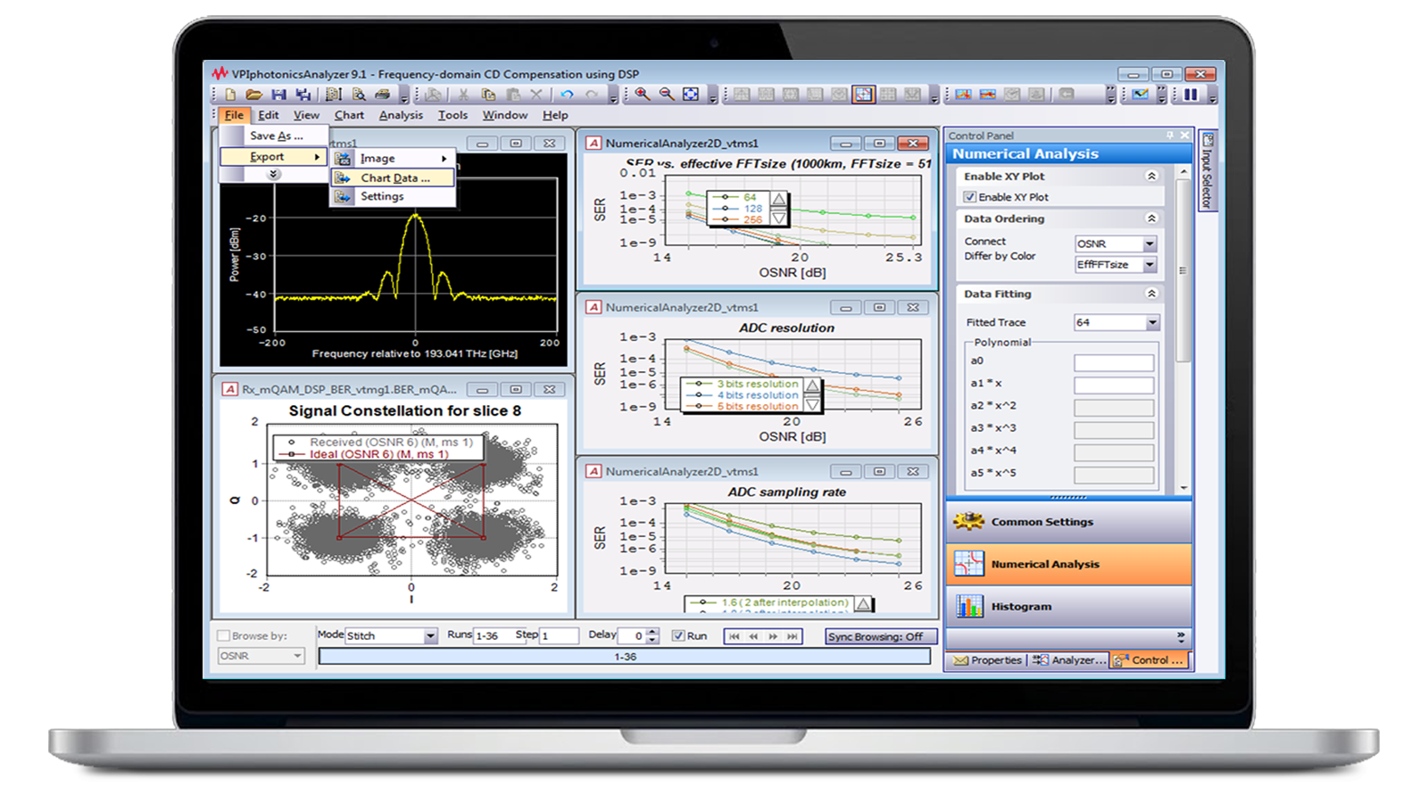
This brochure presents Keysight’s VPIphotonics portfolio for end-to-end photonic design automation. It covers tools for integrated photonic circuits, optical devices, fiber amplifiers and lasers, transmission systems, and network planning. Key capabilities include interactive simulation, automated optimization, scripting, accelerated computing, and data visualization. Interfaces with third-party software and laboratory equipment support collaborative workflows, while protected model sharing enables design exchange without exposing proprietary information.


blogs
Completing Keysight's End-to-End Photonic Design Workflow
Brochures
Advanced Signal Processing & Analysis for the Laboratory

Brochures
Design of Photonic Systems & Networks
Brochures
Design of Fiber Amplifiers & Lasers
Brochures
Design of Photonic Integrated Circuits
Have Questions? We've Got Answers
Photonic Simulation Environment (VPIphotonics Design Suite) is an integrated photonic design automation platform that combines multiple simulation environments for component, circuit, system, and laboratory-based photonic design workflows.
The suite integrates Optical Transmission System Simulation (VPItransmissionMaker Optical Systems), Test Signal Generation and Analysis (VPIlabExpert),Fiber Amplifier and Laser Simulation (VPIcomponentMaker Fiber Optics), and Photonic Integrated Circuit Simulation (VPIcomponentMaker Photonic Circuits) within a shared software environment.
The platform supports photonic device designers, PIC engineers, system architects, researchers, and technical teams responsible for developing and validating advanced photonic technologies.
Photonic design automation streamlines workflows, promotes reuse of engineering knowledge, reduces manual effort, improves collaboration, and accelerates the transition from research through product development.
By enabling comprehensive simulation, optimization, performance analysis, cost evaluation, and validation within a single environment, teams can identify issues earlier and make more informed design decisions.