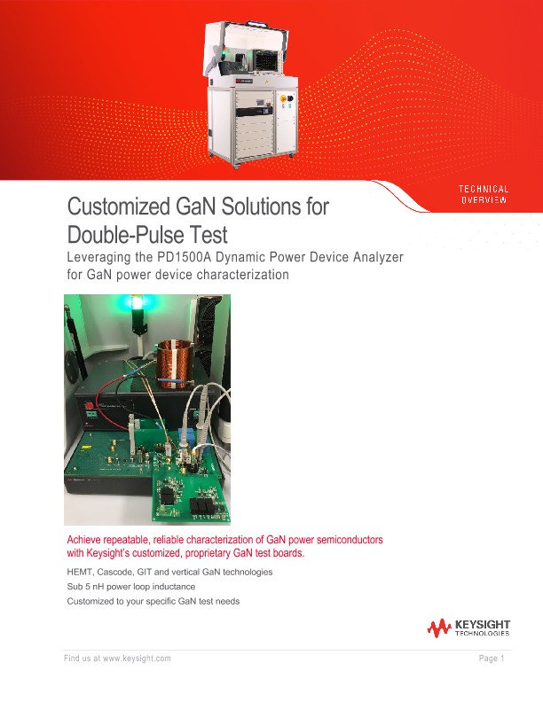
Customized GaN Solutions for Double-Pulse Test
Technical Overviews
Introduction
Keysight Technologies introduced the PD1500A dynamic power device analyzer and Double-Pulse Tester (DPT) in 2019 to address wide bandgap (WBG) dynamic test and characterization requirements. Before then, commercially available dynamic power device test systems were developed for slower silicon (Si) power FETs, focusing on resistive switching techniques. Unfortunately, they are inadequate for characterizing the faster switching speeds and edge rates of WBG devices, which forced power semiconductor manufacturers and power device designers to develop custom characterization solutions.
Because there are many factors (e.g., inductive switching, power loop parasitics, gate driver design, etc.) that affect dynamic parameter results, testing of these WBG devices evolved into a situation where power device manufacturers and consumers can’t easily compare their results.
The major objective of the PD1500A is to provide repeatable and reliable characterization results for WBG devices. Whether it is from person-to-person or system-to-system, one achieves a consistent comparison of different power devices allowing you to determine the best power device for your design. The initial PD1500A introduction in 2019 was focused on Si FETs, IGBTs, and SiC FETs. Its modular architecture minimized the need for customization of the test solution. Since introduction the PD1500A has demonstrated repeatable and reliable results for these power semiconductors.
GaN FET Test Challenges
Because GaN FET switching speeds and edge rates are up to 10 times faster than SiC, additional challenges are encountered when designing a DPT system that provides repeatable and reliable characterization results
• Variety of device designs and form factors – The industry is still developing different topologies and approaches to maximize the benefit of GaN power devices. Therefore, there is less standardization in devices, requiring more customized designs.
• Stable DPT operation – Minimizing power loop and gate loop inductance is even more critical for the high-frequency energy in the GaN switching waveforms. Otherwise, you can easily have excessive ringing causing HV oscillation, which frequently leads to the destruction of the device or damage to the test system
• High bandwidth, low parasitic current measurements – Because of GaN’s high-frequency energy in the switching waveforms, it is important to have a higher frequency and a lower parasitic current measurement capability.
• Dynamic Rds(on)/Current Collapse – Unlike Si and SiC power device, GaN FET has dynamic Rds(on) characteristics due to a charge trapping phenomenon within the crystal/dielectric film or the interface between the dielectric and the semiconductor layer.
• DUT connection to system – The GaN FET connection to the test system is also a parasitic that must be minimized. Soldering the device is ideal from a parasitic perspective but is difficult to use and time-consuming when testing many devices.