
Transforming Chaos Into Clarity: Keysight Data Management for the AI Era
Learn how Keysight SOS data management boosts global semiconductor design with AI-driven engineering intelligence, governance, and traceability.
Key takeaways:
- For chip design driven by artificial intelligence (AI), effective data management must be in place to train the AI models and agents.
- Designing novel AI accelerator chips for mixed-signal and high-speed digital design uses requires data management with flexible metadata capabilities.
- Keysight SOS is a powerful data management platform that facilitates AI-powered chip design workflows and AI accelerator designs.
Keysight’s SOS platform transforms semiconductor design workflows by reducing productivity loss, improving global collaboration, and ensuring IP traceability across the lifecycle. With deep electronic design automation integration and intelligent data management, SOS aligns design management (DM) and design verification (DV) to support the rapid growth of AI and analog/digital (A/D) markets.
In this article, learn about Keysight solutions for semiconductor data management in the AI era.
How is state-of-the-art AI assisting in chip design workflows?
Artificial Intelligence (AI) techniques, machine learning models, and AI agents are fundamentally transforming chip design and electronic design automation workflows. They require integrated circuit (IC) data management tools as outlined below.
How are large language models (LLMs) useful for chip design?
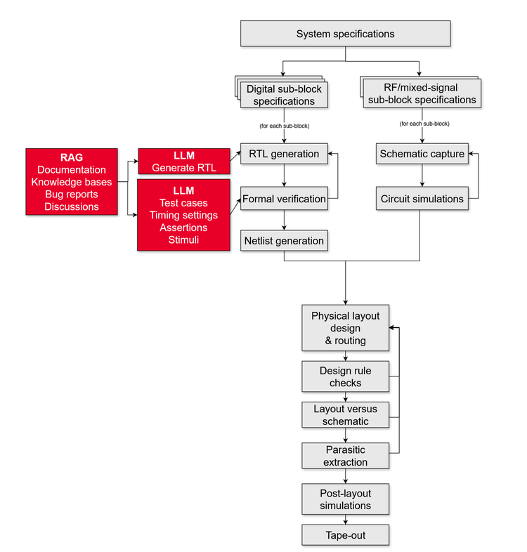
Figure 1. LLMs in chip design
LLMs are being used for natural language processing, code generation, and DV tasks. The table below describes them along with relevant data management (DM) concerns.
- support LLM fine-tuning since RTL is specific to industry, function, and use case
- retrieve specifications and code for training datasets
- create test cases
- generate timing settings
- create assertions
- generate stimuli (conditions and inputs)
- retrieve correct versions of specifications and RTL
- efficiently store large DV artifacts
- support MLOps in electronic design automation (EDA)
- use existing documentation and curated knowledge bases to improve correctness
- enable storage, querying, and retrieval of unstructured data like documentation, knowledge bases, discussions, bug reports, enterprise data, and external data sources
How is agentic AI facilitating chip design?
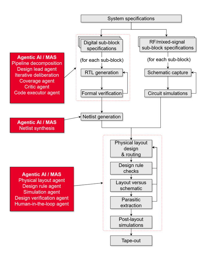
Figure 2. Agentic AI for chip design
Agentic AI and multi-agent systems (MAS) are good at autonomously iterating over end-to-end workflows. They overcome the limitations of standalone LLMs. Chip design lends itself to this incremental autonomous improvement using agents, as shown in the following table.
- break down chip design into small tasks
- execute using specialist AI models
- retrieve information for decision-making by agents and AI tools
- iteratively refine designs
- review previous results
- identify errors (counterexamples in formal verification)
- store, version, and retrieve large artifacts with low latency
- generate microarchitecture and RTL from natural-language requirements
- store requirements under version control
- provide coding standards and linting rules
- run RTL simulators
- execute co-simulation tools
- analyze correctness
- run formal verification tools
- monitor code coverage
- supply data and ancillary knowledge demanded by the agents
- analyze static timing
- generate corrections
- resynthesize
- store intermediate and final netlists for traceability
- transform verified RTL to physical layout
- run EDA tools
- optimize power, performance, and area
- handle gigabyte-sized physical design files
- improved floorplanning and routing using historical knowledge
- allow design engineers to resolve ambiguities and errors
- chronicle all ambiguities, errors, and decisions for triaging, traceability, and institutional memory
How is data management critical to AI-powered chip design and EDA?
A major challenge for AI in EDA is the vast, complex, and often fragmented nature of chip design data. AI success is dependent not just on the model and agent capabilities, but also on supplying clean, connected, and contextualized data to them.
We explained the key demands on the DM in the previous sections. From them, we can infer the capabilities of an ideal AI-ready infrastructure for semiconductor design:
- Structured and contextualized data: DM must support high data quality with relationship tracking, dependency mapping, and design hierarchy for every intellectual property (IP) block. Contextual metadata like the process node, verification history, and usage footprint must also be maintained.
- Unified data ecosystem: AI will be increasingly integrated into radio frequency (RF), mixed-signal, and A/D applications like telecom base stations. SOS provides a unified engineering data ecosystem for AI and A/D markets. It is one of the most powerful RF and high-speed digital design collaboration platforms. SOS also facilitates EDA tool integration for analog/mixed-signal design with platforms like the Advanced Design System.
- Traceability: DM must link every IP block to its lineage and trace back test results and coverage metrics to design changes.
- Scalability and performance: DM must handle large binary design files efficiently, which regular file storage and software version control systems (VCS) are unable to do.
- IP reuse and traceability in SoC development: DM must store searchable metadata and usage context to enable AI recommenders to suggest pre-verified IP blocks for reuse in new designs.
- Predictive verification: AI can identify failure patterns by linking test data, design versions, and change history, allowing engineers to receive early alerts and identify root causes faster. DM is essential for such data linking.
- Layout suggestions: AI learns from historical design records supplied by the DM to propose constraint blocks, floor plan proposals, or routing strategies with awareness of dependencies and process rules.
- Design rule enforcement: AI uses records of prior violations and fixes supplied by the DM from previous projects.
How does Keysight SOS support AI-driven verification and validation workflows?
Keysight SOS is a modular data management platform crafted to meet the evolving needs of semiconductor design teams of all sizes, from small agile teams to globally distributed enterprises.
Keysight SOS combines proven semiconductor-grade reliability with modern scalability and intelligence. Whether you're managing a single project or coordinating global teams, SOS empowers you to treat design data not just as files but as a connected, strategic asset.
With industry certifications, deep data integration with EDA tools, and AI readiness, it’s the ideal platform for organizations ready to move from control to insight. Keysight SOS is a fully AI-ready DM. With Keysight SOS, minimize productivity loss from manual data handling, which wastes 63% engineering time.
In the following sections, we explain all its AI-friendly capabilities.
What are the bundled editions of Keysight SOS?
The Keysight SOS platform for semiconductor engineering comes in two bundles:
- SOS Core: This provides all the high-performance DM core features.
- SOS Enterprise: This adds IP management (with a standardized catalog to find, compare, and reuse assets), secure global collaboration, governance, and AI-ready infrastructure to SOS Core.
Let's understand each bundle in more detail.
What is SOS Core?
With version control capabilities, built-in metadata capture, integration into EDA workflows, and collaboration mechanics, SOS Core enables efficient concurrent engineering and accelerates IC design.
SOS Core delivers fast, reliable access to large design datasets without the need to clone entire repositories on each workstation.
It’s scalable by design. A smart client-server architecture minimizes storage and network load by fetching only the data needed.
It deeply integrates with all the leading EDA environments. Engineers can manage versions, track changes, and compare schematics and layouts from within their preferred EDA environments.
AI and agentic workflows are supported. It's ideal for small to mid-sized teams planning on AI-assisted IC design and also offers a seamless upgrade path to the Enterprise edition.
What is SOS Enterprise?
SOS Enterprise is an end-to-end semiconductor IP lifecycle management software that enables secure, global collaboration for large, distributed organizations. It extends SOS Core with global-scale governance, security, and lifecycle traceability.
It unifies design data, IP relationships, and verification results under a single system of record — ensuring every change is tracked, every dependency is visible, and every asset is audit-ready.
With role-based data access control, compliance automation, and integration with PLM, ERP, and issue-tracking systems, it connects engineering data to the broader product lifecycle.
Its structured metadata and application programming interfaces (APIs) enable AI and machine learning workflows, transforming engineering data into a foundation for intelligent automation and accelerated innovation.
How do Keysight SOS metadata features support AI-assisted EDA?

Figure 3. Keysight SOS design hierarchy
Keysight SOS stores all artifacts related to a chip design in centralized repositories. These include requirements, specifications, RTL code, intermediate design files, tapeout files, technical documents, embedded software development, simulation models, testbenches, legal documents, and regulatory reports. Any amount of metadata can be added to each artifact.
All these artifacts and metadata can be queried by AI agents and LLMs through the API endpoint provided by SOS.
For high performance and scalability, all the data of a project is not downloaded to a workstation or AI host. Instead, only the directory tree and symbolic links to files are created locally. The actual data of a file is downloaded only on demand when a tool wants to read it.
How does Keysight SOS manage chip designs across global semiconductor teams?

Figure 4. SOS version control integrated with an EDA tool
Keysight SOS enables productive semiconductor design and real-time collaboration between globally distributed teams. It does this through the following capabilities:
- Integrated version control: SOS is a DM with integrated version control for chip design and verification. This enables multiple teams and engineers to work simultaneously on the same project on different components, sync up their changes, and test or simulate the entire device.
- Change propagation: Keysight SOS deploys data efficiently in a hub-spoke model with a central repository and multiple cache servers, one at each design site. All teams anywhere in the world see the same version and branch history. All teams can work on the same version concurrently.
- Version information: SOS shows the version number of an active file in all supported EDA environments. This enables engineers to ensure that they're always working on the correct version of a design.
- Design hierarchy awareness: SOS treats a directory tree as a device hierarchy without any special setup or custom scripting. If a team changes a subcomponent, it triggers automated rebuilding, testing, and verification of all ancestor components one by one up the hierarchy.
- Usage tracking: SOS shows all the design projects that depend on a selected IP block or subsystem. This enables changes to be propagated across projects. It also facilitates organization-wide IP reuse and breaking down of data silos by showing projects that are already using an IP block.
- Secure collaboration tools for global semiconductor teams: While facilitating collaboration and knowledge exchange, SOS does not compromise security and IP protection. Built-in access control allows sensitive data to be shown only on a need-to-know basis.
- Regulatory and standards compliance: SOS has built-in traceability for every change and artifact. This is essential to strengthen governance and auditability in regulated environments. Defense and aerospace companies can comply with U.S. International Traffic in Arms Regulations. Using SOS, medical device companies can more efficiently adhere to the International Organization for Standardization (ISO) 13485 quality management and ISO 14971 risk management standards. For automotive functional safety, SOS is one of the best data management solutions for ISO 26262 compliance.
- Engineering data governance for regulated industries: SOS provides effective data governance features for industries like defense and health care.
- Visual design tools: SOS includes Visual Design Diff, a tool to view schematic and layout changes visually between versions and design variants regardless of the environment or tool used for the change.
What are the storage and network savings when using Keysight SOS?

Figure 5. Chip design data volumes
Keysight SOS is designed to optimize network and storage use. This not only reduces network and storage utilization but also reduces latencies due to far fewer network and file operations.
For optimized storage, SOS avoids the massive data duplication inherent in traditional VCS. When a project is cloned in other systems, all files are downloaded to the local system. This is highly inefficient for chip design projects that typically involve gigabytes-sized binary files.
In contrast, SOS deploys a local cache server at each site and uses smart caching strategies to optimize storage and network utilization. When a project repository is cloned to a user workspace, SOS creates only its directory tree and symbolic links to files. Data for the active version of a file is downloaded from the cache server only when some component or tool wants to read it. This drastically reduces total storage and network utilization. The local copy of a file is scrubbed after a commit to further reduce storage.
This copy-on-demand also results in significantly reduced latencies. The user experience for design engineers remains responsive and snappy.
How does Keysight SOS differ from Git, Perforce, or Subversion for IC design?

Figure 6. SOS versus other VCS
Keysight SOS is specifically architected to handle large files and big volumes of data while avoiding data duplication and network strain, which tracks exceptionally well for chip design projects. Its key differences from other VCS are outlined below.
Component dependency awareness
Traditional VCS uses directories and files but doesn't assume any dependencies in a directory tree. A subcomponent change does not trigger any kind of verification of parent components. For a chip design project, this creates an unacceptable risk of errors. Dependency-based triggers have to be manually set up and maintained, both of which involve engineering effort.
In contrast, Keysight SOS is aware that most chip designs involve hierarchies, especially SoC design projects. It treats subdirectories as dependencies. When a subcomponent design changes, it automatically triggers rebuilds, simulations, tests, and verifications for all the ancestor components. Every change is propagated and verified up and down the device hierarchy.
Optimized for binary file storage
Another key characteristic of chip design projects is the large number of heavy binary files managed by EDA tools.
Traditional VCS like Git are designed for software code in plain text format. Their user experience for managing binary files is clunky. Their storage and network operations are not optimized for large binary files.
Unlike them, SOS version control does not download all files to the local machine. It just recreates the directory tree and creates a symbolic link for each file. The contents of a file are downloaded only on demand. This reduces both disk and network utilization compared to other VCS.
Efficient network utilization
To reduce network latencies, on-demand downloads are fetched from a local cache server, not the central repository. This efficient architecture enables intense real-time collaboration between globally distributed sites in large semiconductor enterprises. Committed changes are first uploaded to the local cache server and then synced with the central repository.
Seamless integration with EDA tools
Unlike traditional VCS, Keysight SOS is deeply integrated with all the popular EDA tools used by IC engineers. Version control, storage management, and change propagation are all directly available in the user interfaces and workflows of these tools. These EDA integrations are listed in the next section.
Which EDA tools integrate with Keysight SOS?
Keysight SOS integrates with all the leading EDA tools like:
- Advanced Design System
- Cadence Virtuoso Studio
- Synopsys Custom Compiler
- Synopsys Laker
- Siemens EDA (Pyxis)
- Siemens EDA (Tanner)
- Empyrean Aether
- MathWorks MATLAB
- Silvaco Gateway
Adopt Keysight data management for the AI era
A platform like Keysight SOS streamlines chip data management and provides a competitive advantage to semiconductor companies by reducing time-to-market.
Contact us for technical assistance and demos in adopting Keysight SOS for your chip projects.
Related Posts