Confirme o seu país ou área
Por Favor, Confirme
Confirme o seu país para ter acesso a informações sobre preços aplicáveis, ofertas especiais, eventos e contatos.
O que você está procurando?
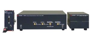
E4727B Advanced Low-Frequency Noise Analyzer
Get a deeper, closer look at low frequency noise with the A-LFNA integrated with WaferPro Express, featuring data analysis, wafer prober control and test suite automation.
A partir de
Highlights
- Advanced low-frequency noise analyzer’s integration with PathWave WaferPro (WaferPro Express) enables turnkey noise measurements as well as measurement of DC characteristics, capacitance and RF S-parameters
- Extremely low device noise measurement such as transistor linear region noise by newly designed LNA
- State of the art new LNA also allows noise measurement in very low bias current
- High power device noise measurement even in the high current like 1A
- Improve measurement productivities by fast measurement speed even in the high accurate condition with number of averaging
- Software module measures DC characteristics, 1/f noise, random telegraph noise and conducts data analysis
- Keysight’s close collaboration with FormFactor enables a complete integrated on-wafer solution with automated control of all major wafer probing systems
The E4727B Advanced Low-Frequency Noise Analyzer enables fast, accurate and repeatable low-frequency noise (LFN) measurements on numerous device types. Now, thanks to tight integration with PathWave WaferPro (WaferPro Express) software, device modeling and characterization engineers can now add noise measurements to a larger suite that includes high-speed DC, capacitance and RF S-parameter measurements, all the while automating wafer prober control.
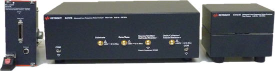
Figure 1: The new E4727B Advanced Low-Frequency Noise Analyzer (A-LFNA).
Applications
The applications are numerous; however, a few important ones are listed as follows.
- Process design kit (PDK) development - Semiconductor device foundries enable fabless design centers to design components such as transceivers for mobile phones, frequency synthesizers, analog-to-digital converters and much more. To make this possible, the foundries must provide PDK’s with simulation models of the primitive devices. The simulation models must include noise effects on transistors (BJT, CMOS, etc.) and resistors. The noise models must be across all possible bias currents, temperatures and device geometries.
- Manufacturing statistical process control and reliability - As an example, manufacturers of GaN devices may use noise measurements across their wafers as an early indicator of device reliability. Those devices that exhibit more noise are likely to fail sooner. Now we have a nondestructive way of assessing reliability, quite in contrast with standard accelerated life testing. Furthermore, for circuit applications where noise is a critical parameter, wafer level measurements may be used to track the evolution of noise performance across days, weeks and months of manufacturing.
- IC noise specification - Integrated circuit manufacturers of operational amplifiers and linear voltage regulators often need to characterize input referred voltage noise as a critical specification in their datasheets; one wafer may contain >10 thousand such circuits. To efficiently measure and map circuit performance across the wafer (and even across lots of wafers), the probe and signal conditioning circuitry must be placed close to the device under test to improve grounding and minimize external noise influences.
Turnkey Measurements
The A-LFNA’s built-in measurement routines make DC and noise measurements turnkey. For example, to measure noise on an N-Type MOSFET, the system automatically chooses the source and load impedances that will best expose the intrinsic device noise. The engineer can accept these recommended settings or make changes, and a noise measurement is initiated. The A-LFNA then measures noise power spectral density (1/f noise) and noise in the time domain (RTN). Resulting data is plotted using a multiplot data display window. Various windows' tabs help facilitate common tasks such as evaluating device DC operating point and measuring the slope of the power spectral density curve. Noise data can also be analyzed and represented in device models using device modeling tools such as PathWave Model Builder (MBP) and PathWave Device Modeling (IC-CAP). Circuit designers can use these device models to ensure highly accurate RF and analog low-noise circuit design.
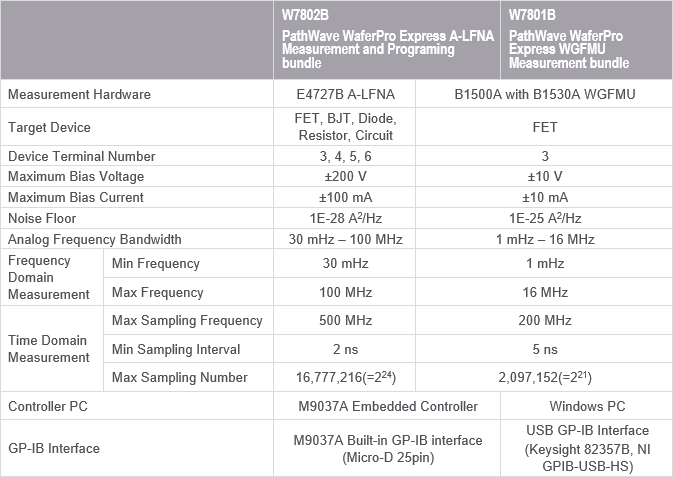
Automated RTN Solution Using W7801B and B1500A
W7801B (PathWave WaferPro Express WGFMU Measurement bundle) efficiently performs at a low cost an automated RTN measurement on the wafer using the B1500A Semiconductor Device Analyzer with the B1530A Waveform Generator/Fast Measurement Unit (WGFMU). It can improve the efficiency of RTN measurement and data analysis including wafer prober control.
Key features
- Automated measurement without programing
- Auto prober control
- Wafer mapping
- Single data display for multi decade in frequency domain
- Upgradeable from your existing B1500A
RTN and 1/f Noise Measurement System Comparison
Measurement Examples
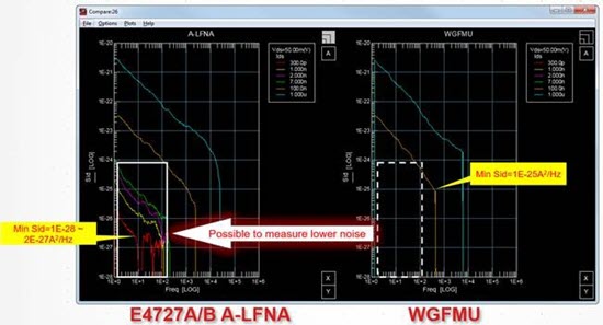
Figure 2. Example of WGFMU measurement.
For more information on WGFMU, please see the links below.
Principais especificações

Interested in a E4727B?
Extend the capabilities for your Advanced Low-Frequency Noise Analyzer
Featured Resources for E4727B Advanced Low-Frequency Noise Analyzer


Related Products
Want help or have questions?
- © Keysight Technologies 2000–2024
- Privacidade
- Mapa do site
- Termos
- Trademark Acknowledgements
- Contate o Webmaster