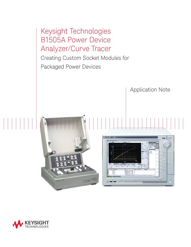
The Keysight Technologies B1505A Power Device Analyzer/Curve Tracer is a total solution for power device measurement, providing superb measurement accuracy and resolution, high voltage and current sourcing capability (up to 3000 V and 20 A), and an easy-to-use MS Windows based software environment.
Measurement environment safety is extremely important for power device characterization because the high voltages and currents used can cause serious injury and are even potentially fatal. To prevent this Keysight offers the N1259A packaged part test ixture for use with the B1505A. The N1259A is equipped with an interlock function that does not allow the B1505A to force more than 42 V unless the ixture lid is closed.
Keysight also supplies an inline package socket module (N1259A-010) with the N1259A that allows you to measure TO-220 and TO-3P type packaged power devices safely.
However, although these package types are widely-used for power devices, surface mount device (SMD) style packages are becoming increasingly popular for power transistors. Obviously, the N1259A-010 socket module cannot be used to test these types of power devices.
To meet this need, the Keysight B1505A also supports the universal socket module (N1259A-011) shown in figure 1.
The N1259A-011 allows you to develop a custom socket module to measure the package type of your choice.
This product note describes the procedure to develop custom socket modules to measure packaged power devices other than TO-220 and TO-3P with the Keysight B1505A.
Custom socket module development overview
The following items are required for custom socket module development.
- Universal socket module
- Test socket
- Printed circuit board
The test socket used to hold the test devices is mounted on a printed circuit board. The printed circuit board transfers the voltage and current from the universal socket module to the test socket, and it is mounted onto the socket module as shown in figure 2.
Obviously, you irst need to obtain the proper test socket for your device. Besides having the correct form factor, the test socket must be able to withstand the current and voltage that you intend to apply to your device. Once you have selected a test socket, you need to design and fabricate a printed circuit board to accommodate it.
Note that if you do not need to apply 3000 V to your device then you can purchase a test socket with a lower voltage handling capability. The B1505A has the capability to limit voltage and current output, so you can prevent inadvertent damage to your test socket and device. This feature will be described later in this product note.
Printed circuit board development
As previously mentioned, a custom printed circuit board is required to interface between your test socket and the universal socket module. The printed circuit board must also have the ability to withstand high voltages and currents. Therefore, when developing a printed circuit board the board size/material, clearance/creepage distance and boring/ patterning must all be taken into account.
Board size/material
To it the universal socket module, the printed circuit board must be 90 mm x 105 mm with a preferred thickness of 1.6 mm as shown in igure 3. In addition, the board material should be able to withstand high voltage. In the example shown in this product note, the material used to construct the board was Panasonic R-1755C.
Clearance/creepage distances
You must also consider clearance and creepage distance of the patterns on the printed circuit board for high voltage testing. Clearance is deined as the shortest distance between two conductive parts as measured through the air; creepage is deined as the shortest distance between two conductive parts as measured along the surface of the insulation. For 3000 V a clearance of at least 5 mm and a creepage of 16 mm are necessary according to international safety standards IEC 60065 and IEC 60664. In cases where the available space makes it dificult to maintain the speciied creepage distance, slits can be used to eliminate direct paths between conductive components and thereby increase the effective creepage distance. Figure 4 shows an example where slits are used to meet the speciied creepage distance.
Boring/patterning
The actual circuit board creation should be performed by a company that specializes in this type of work. There are many companies located throughout the world that will handle these types of small jobs.
The Keysight B1505A provides an inline package socket module for TO-220 and TO-3P type packaged power device measurement. Although this socket module supports many power devices, other package types (such as SMD) are increasing in popularity and you may have the need to measure them.
Keysight provides a universal socket module to support the testing of other power device package styles. This allows you to test virtually any type of packaged power device, with the only requirement being that you need to supply the correct test socket and printed circuit board. This product note has described the procedure for doing this, as well as covering how to test the socket after construction for leakage and how to prevent inadvertent damage to the socket using the SMU output setting limitation feature.
Oscilloscopes
Analyzers
Meters
Generators, Sources, and Power Supplies
Software
Wireless
Modular Instruments
Network Test and Security
Network Visibility
Services
Additional Products

