Insufficient measurement capability
Power devices require characterization across their entire operating region, ranging from nano amps or microvolts up to more than one thousand amps and thousands of volts. In addition, the ability to perform narrow (microsecond range) pulsed IV measurements is also essential to prevent device self-heating, which can distort measurement results. Lastly, characterizing the switching speeds of power devices necessitates some means to characterize gate resistance (Rg), gate charge (Qg), and junction capacitances at biases of several thousand volts. These parameters have become extremely important as end-application switching frequencies have continued to increase. However, traditional measurement equipment cannot meet all of these requirements.
Verification of power device reliability
Since many power devices are used in harsh environments and mission-critical applications, they have to be highly reliable. Characterizing performance under a wide range of operating temperatures as well as near the safe operation area (SOA) is crucial to meeting reliability targets. Unfortunately, temperature testing is time-consuming, complex, and prone to oscillation issues caused by long cables when an external thermal chamber is used. SOA testing typically requires dynamic testers, which are difficult to use and lack sufficient accuracy
Issues with novel new device (SiC, GaN, Ga2O3, IGBT) characterization
New wide-bandgap materials such as SiC, GaN, and Ga2O3 show great promise for emerging high-power applications because of their ability to withstand large voltages and their fast switching speeds. IGBTs are becoming increasingly important as electronic switches for a variety of applications. Characterization of large breakdown voltages (up to 10 kV), high currents (hundreds of amps), gate charge, junction capacitances under high voltage DC biases (up to 3000 V), device temperature dependency, and the GaN device current collapse effect are measurement capabilities that are crucial to bringing these new devices to market as quickly as possible.
No curve tracer hardware support or feature enhancements
Until recently, curve tracers have been the de facto standard tool for power device evaluation. However, conventional curve tracers do not possess the abilities necessary to evaluate modern power devices. They lack crucial capabilities such as transfer curves or junction capacitance characterization, cannot generate sufficiently short pulse widths, and possess insufficient accuracy. Extracting PC-compatible data from curve tracers is also inconvenient and time-consuming.
Safe and efficient packaged device testing
A test fixture that is both safe and easy to use is crucial for packaged power device evaluation. However, the lack of a standard test fixture for high-power devices has forced many people to create their own solutions, which become challenging to manage when multiple package types need to be tested. Moreover, temperature-dependent testing (which is mandatory for power device evaluation) cannot be done safely and reliably.
Power device development costs
The ability to probe devices on-wafer significantly saves both time and money by eliminating the need to package the devices beforehand. However, on-wafer power device measurements have previously not been easy to make. Not only the time and cost of supporting the on-wafer measurement environment but also the safety of the on-wafer measurement environment are big concerns.
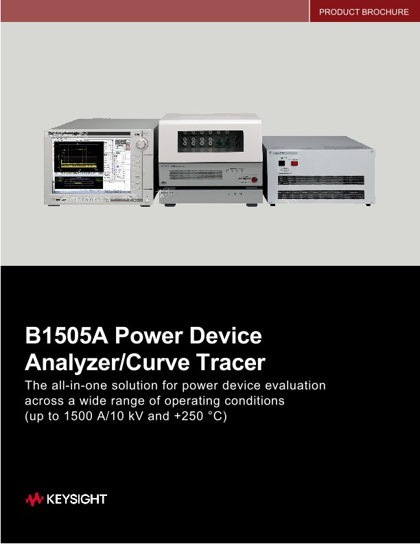
The B1505A meets the measurement challenges posed by state-of-the-art power devices. It is the only single-box solution to accurately evaluate and characterize power devices from sub-picoamps up to 10 kV and 1500 amps. It can also measure dynamic parameters such as gate charge and capacitance at 3000 V of DC bias. It supports thermal testing from -50 °C to +250 °C.
In addition to these impressive measurement capabilities, the intuitive EasyEXPERT group+ software environment makes data analysis a snap. You can also easily export data into your PC-based work environment and use this data to generate presentations and reports.
The B1505A supports two standardized test fixture solutions, the N1259A, and the N1265A, that are differentiated by their voltage and current ranges. Both solutions are compatible with a variety of different socket types. The B1505A also supports on-wafer testing of power devices, thereby eliminating the need to package the devices first. This capability dramatically improves the turn-around time (TAT) when testing devices in the lab.
Taken together, these capabilities and features result in revolutionary efficiency improvements in power device evaluation and a significant reduction in the cost of tests
Keysight B1505A Key Feature Summary
Precision measurement across a wide range of operating conditions
- All-in-one solution for power device characterization up to 1500 A/10 kV
- Medium current measurement with high voltage bias (e.g., 500 mA at 1200 V).
- μΩ resistance measurement capability
- Accurate sub-picoamp level current measurement at high voltage bias
- Fully automated, safe, accurate, and fastest available thermal testing from -50 °C to +250 °C
Extensive device evaluation capabilities
- Fully automated Capacitance (Ciss, Coss, Crss, etc.) measurement at up to 3000 V of DC bias
- High-power pulsed measurements down to 10 μs
- Both packaged device and on-wafer IGBT/FET gate charge measurement
- High voltage/high current fast switch option to characterize GaN current collapse effect
- Up to five high voltage (3 kV) source/measure channels for maximum flexibility
- Safe temperature-dependent testing via an interlock-equipped test fixture
- Supporting SiC MOSFET Vth, BTI-Vth measurements based on the JEDEC standards
Improved measurement efficiency
- Switch between high-voltage and high-current measurements without the need to re-cable
- Automatic test circuit formation for transistor junction capacitances (Ciss, Coss, Crss, Cgs, Cgd, Cds, etc.) for both packaged and on-wafer devices
- Standard test fixtures with interlock for safe packaged power device testing
- Supported and secure on-wafer high-power testing over 200 A and up to 10 kV
- The Oscilloscope view allows verification of applied voltage and current waveforms
- MS Windows-based EasyEXPERT group+ software facilitates data management and analysis
Upgradable and scalable hardware architecture
- A wide selection of measurement modules
- Support for high-power devices with up to 6 pins
Oscilloscopes
Analyzers
Meters
Generators, Sources, and Power Supplies
Software
Wireless
Modular Instruments
Network Test and Security
Network Visibility
Services
Additional Products

