Confirm Your Country or Area
Please Confirm
Confirm your country to access relevant pricing, special offers, events, and contact information.
What are you looking for?
Keysight x1149 supports Intel ® Silicon View Technology
Test Access
Electrical test, unlike imaging test, requires physical connection to the nets of the electronic circuit to provide the stimulus and measure the expected results. The physical connection is the test access made using a test probe contacting a test pad of the net on a printed circuit board assembly (PCBA). Electrical test has the advantage of validating the electrical path of a net regardless whether the trace and solder joint on the PCBA is visible or hidden. Examples of hidden solder joints are ball grid array (BGA) or microBGA IC packages, the preferred IC packaging for System-on-Chip(SoC) devices like central processing unit (CPU).
Test access can be reduced as PCBA density increases to accommodate:
- Shrinking form factors
- Less sockets as more devices are soldered down (CPU, Memory)
- IC package on IC package assembly
- Increasing bus speeds
- High density interconnect(HDI) for soldered down LPDDR3 memory
- Cost pressures
Alternative test access methodology like Keysight Bead Probe Technology can be deployed to recover test access. Unlike traditional test pads, Bead Probe has the advantage of requiring almost no additional real estate and can be placed on high-speed traces without affecting signal fidelity1.
Limited Test Access
IEEE 1149.1, commonly referred to as Boundary Scan, is a reliable test methodology to identify the IC package and validate the connectivity of the IC package to the PCBA. Boundary scan only requires test access to four pins of the IEEE 1149.1 test access port(TAP) regardless of the number of pins of the IC package. It is a very efficient and productive test methodology for ultra large scale integration (ULSI) devices like SoC.
Boundary scan capability is available on Keysight’s i3070 in-circuit tester (ICT), i1000D ICT and the x1149 Boundary Scan Analyzer. The x1149 has the smallest footprint and incorporates Keysight’s innovative boundary scan test extensions maximizing test coverage with Silicon Nails and Cover-Extend Technololgy(CET).
Intel® Silicon View Technology
And now Keysight is adding Intel® Silicon View Technology (Intel® SVT) to our suite of limited test access tools.
Intel® SVT, a proprietary Intel® test technology, enables the test for Haswell CPU designs if test access is constrained by PCBA real estate or high-speed signal fidelity. It requires test access to the debug port2 and uses Intel® DFx* Abstraction Layer (Intel® DAL) to securely access the Haswell CPU silicon to verify its function and that of surrounding devices.
Intel® SVT requires the BIOS to be set up according to Intel® BIOS Writer Guide3, reserving a designated register to host the results of the Intel® SVT test. During manufacturing test, the PCBA under test has to be powered up safely to run the BIOS and Intel® SVT will post the results of its test into the designated register. The content of the register is then compared to known good board values to assess whether the PCBA passes or fails the set of tests.
Intel® SVT will test via the Haswell CPU (and BIOS) the:
- Platform hub controller (PCH)
- Memory
- Graphics eg VGA, HDMI, eDP
- High speed I/O(HSIO) eg PCIe, SATA, USB3
- Communication interfaces eg LAN, USB2
- I/O Peripherals eg keyboard, audio
Keysight’s solution using Intel® SVT
Test access, either traditional test pads or Keysight Bead Probe, will be available for every Haswell CPU design, be it 10% or 90% of the total nets. In-circuit test should be implemented for nets with available test access to ensure these nets are devoid of open and short and the components loaded are correct. Preferably these nets should include power and ground nets to increase the confidence of successfully sequencing power to the PCBA prior to Intel® SVT test. Test access challenged designs should prioritize test access to the debug port, power and ground nets and critical components.
After completing the unpowered in-circuit test, the i3070 ICT, i1000 ICT or x1149 Boundary Scan Analyzer can sequence the power to the Haswell CPU PCBA and measure the on-board voltages. It will shut off the power to protect the PCBA if the on-board voltages are not within the safe limits. After successfully powering up the PCBA, boundary scan tests will verify the solder joints of the CPU(and PCH in 2 chip designs). If a open or short is detected, the test will abort; otherwise it will continue to Silicon Nail and CET tests to validate the memory, sensor hub and high-speed bus using loop-back connectors.
At the completion of these tests, the ICT or x1149 will launch the Intel® SVT tests using Intel® DAL to verify the PCH, memory, graphics and HSIO (USB 3.0, SATA, PCIe,…) and peripherals.
At the conclusion of a successful combined ICT or x1149 with Intel® SVT test, confidence will be high the CPU and peripherals on the motherboard is in good working condition, ready to be assembled into the final product. Figure 1 illustrates a Haswell CPU design and the recommended test strategy with Intel® SVT.
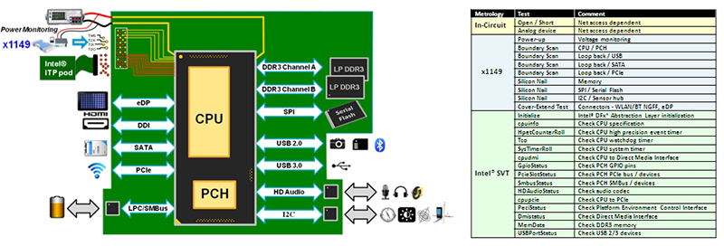
Figure 1: Block diagram of a Haswell CPU design with the deployed test strategy using Intel® SVT.
The flexibility of Keysight’s recommended solution preserves the investment of existing i3070 ICT and i1000 ICT. Alternatively, the x1149 Boundary Scan Analyzer can be paired with Intel® SVT for small footprint requirement. To learn more, request additional product information.
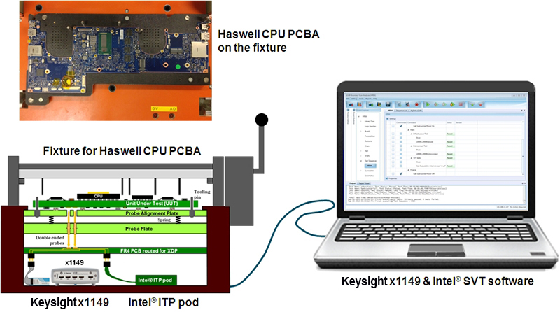
Figure 2: Small footprint solution comprising of a Haswell CPU PCBA fixture, Intel® ITP pod, x1149 Boundary Scan Analyzer and software on a Windows 7 PC.
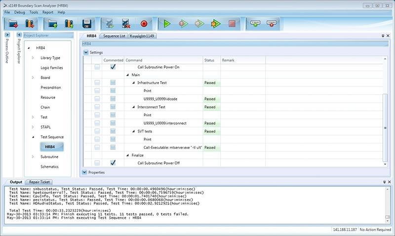
Figure 3: Screenshot of Keysight x1149 and Intel® SVT software test execution.
References
1 Intel course ID # 9492 Manufacturing with Intel® Components - Keysight® Bead Probe Technology MAS
2 Intel document # 479493 Shark Bay and Denlow Platforms – Debug Port Design Guide
3 Intel document # 493770 4th Generation Intel® Core™ Processor Family BIOS Writer’s Guide (BWG)