Confirm Your Country or Area
Please Confirm
Confirm your country to access relevant pricing, special offers, events, and contact information.
What are you looking for?
N7700210C Wafer Prober TAP Plug-In
Easily integrate wafer prober control within TAP test sequences for fully automated wafer and chip scale test solution for Integrated Photonics
Starting from
Highlights
Fully Automated Wafer and Chip Scale Test Solution for Integrated Photonics
Easily integrate wafer prober control within TAP test sequences
- Test steps for optical and electrical probe positioning and alignment
- Support for array / single fiber probes, edge and surface coupling, RF/DC probes and flexible probe orientations (east/west/north/south)
- Automated device stepping and prober status control
- Measurement test plan and device data management (import / export /editing of device coordinates, device meta parameters and test conditions)
Supported wafer probers
- Formfactor CM300xi with Velox Software and Silicon Photonics Tools
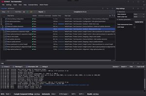
![]() Keysight Test Automation on PathWave (TAP), a modern Microsoft .NET-based application adds workflow sequences through instrument plug-ins without the need for instrument-level programming commands. The N7700210C Wafer Prober plug-in further simplifies automation by handling the interface to the Formfactor semi-automated probe station hardware and Formfactor Velox and Silicon Photonics Tools software. Test steps realize wafer chuck movement, probe positioning, and alignment tasks within a test plan that can be combined with instrument test execution steps. Easy configuration of wafer prober settings for positioning, and for RF and optical probes. Designed for standalone use or in combination with higher level test executive software environments.
Keysight Test Automation on PathWave (TAP), a modern Microsoft .NET-based application adds workflow sequences through instrument plug-ins without the need for instrument-level programming commands. The N7700210C Wafer Prober plug-in further simplifies automation by handling the interface to the Formfactor semi-automated probe station hardware and Formfactor Velox and Silicon Photonics Tools software. Test steps realize wafer chuck movement, probe positioning, and alignment tasks within a test plan that can be combined with instrument test execution steps. Easy configuration of wafer prober settings for positioning, and for RF and optical probes. Designed for standalone use or in combination with higher level test executive software environments.

Keysight’s wafer prober sample test plan with prober steps

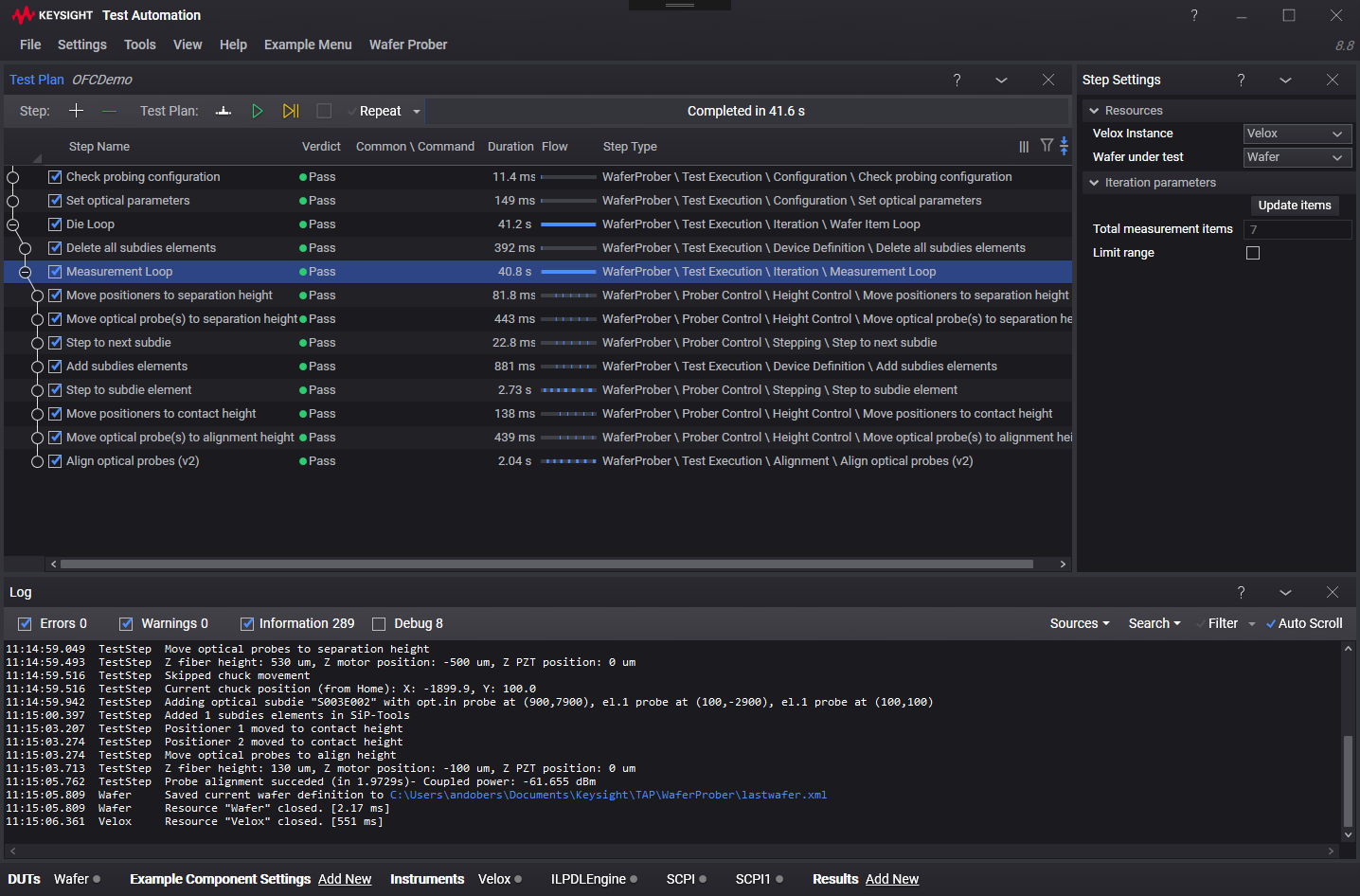
List of device elements and example of element optical IO port characteristics


Free Trials
N7700210C Wafer Prober Plug-In
N7700210C Wafer Prober Plug-In
Interested in a N7700210C?
Extend the Capabilities
Featured Resources


Want help or have questions?