Confirm Your Country or Area
Please Confirm
Confirm your country to access relevant pricing, special offers, events, and contact information.
What are you looking for?
PathWave Device Modeling(IC-CAP)
Complete and accurate measurement control and parameter extraction solution for semiconductor device modeling

Streamline Semiconductor Device Modeling Workflows
PathWave Device Modeling (IC-CAP) software is the industry standard for semiconductor device modeling and characterization. The Integrated Circuit Characterization and Analysis Program (IC-CAP) extracts accurate compact models for high speed/digital, analog, power electronics, and power RF applications. It enables foundries and integrated device manufacturers (IDMs) to streamline semiconductor device modeling workflows for silicon CMOS, Bipolar, compound gallium arsenide (GaAs), gallium nitride (GaN) and many other IC devices.
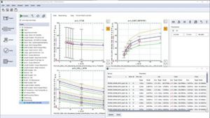
IC-CAP is the one of the most advanced, customizable semiconductor device modeling platform, which includes measurement, simulation, optimization and statistical analysis tools.
- Open device modeling software architecture enhances accuracy and flexibility to create and automate measurement, extraction and verification procedures.
- Turnkey extraction solutions for industry standard CMOS models, such as BSIM3/BSIM4, PSP and HiSIM,. minimize the learning curve and maximize model accuracy.
- Direct links to major commercial simulators ensure consistency between extracted models and the simulators used by circuit designers.

Semiconductor Device Modeling Recentering modeling tool
What's New in IC-CAP 2024
PathWave Device Modeling 2024 features the new Recentering modeling tool helps modeling engineers efficiently adapt existing model cards to new process specifications. It can reduce the semiconductor device modeling extraction time by as much as 70% compared to traditional step-by-step extraction flow.
Learn more
Read the application note
See it in action
How to Extract the ASM-HEMT Model for GaN RF Devices Including Thermal Effects
Gallium Nitride (GaN) high electron mobility transistors (HEMTs) are gaining rapid adoption in high-power, high-voltage, and high-frequency applications due to their superior performance such as high saturation velocity, high breakdown voltage, and high sheet carrier density. However, integrating GaN devices into a circuit design requires accurate and robust circuit simulations. The accuracy of simulations depends on the compact model's ability to predict highly non-linear behavior, including thermal and dynamic memory effects.
Download this application note for a comprehensive extraction procedure for the industry-standard ASM-HEMT model for GaN devices, including self-heating.


Find the Product That's Right for You

See also the W6325B PathWave MBP/IC-CAP Device Model Extraction and W6347B PathWave MQA/IC-CAP Modeling bundles.
Want more information on PathWave Device Modeling Products? View Configuration Guide
End-to-End Semiconductor Device Modeling Solution
Protect Your Innovation Investment


Explore Semiconductor Device Modeling Use Cases


Helpful Resources on Semiconductor Device Modeling


Frequently Asked Questions
Semiconductor device modeling involves creating precise mathematical models that simulate the electrical behavior of semiconductor devices and circuits in response to various stimuli. A device model includes a set of equations with specific parameters or coefficients. Determining parameter values is a meticulous process that involves either direct extraction or optimization techniques to ensure the model equations closely fit the measured data.
Semiconductor device modeling forms the foundation of process design kits (PDKs), offering mathematical models that represent the behavior of the semiconductor devices, such as transistors, diodes, and capacitors, within the integrated circuits (ICs). As semiconductor device sizes shrink to the nanometer scale, device behavior becomes increasingly complicated as new physical phenomena occur. Accurate models enable design engineers to simulate and predict the behavior of devices before moving to costly physical prototyping.
Device modeling falls into the following categories:
- Physics-based models: Engineers recognize physics-based device models for their accuracy, as they rely on fundamental physical laws. One example is the 2D solution of Poisson's equation, which describes the electrical potential distribution in semiconductor devices.
- Empirical models: Derived by fitting equations to experimental data, these models prioritize practical predictability over theoretical foundations. For instance, the Curtice empirical model describes the I-V characteristics of metal-semiconductor field-effect transistors (MESFETs) and high-electron-mobility transistors (HEMTs).
- Semi-empirical models: These models combine physical principles with empirical data. For instance, Gummel-Poon is a semi-empirical model for bipolar junction transistors (BJTs).
- Table-based models: Table-based models, such as the HP Root FET model, interpolate measured data to simulate device behavior under different conditions.
- Artificial neural network (ANN) models: These models use artificial intelligence algorithms to learn from data and predict semiconductor device behavior. For instance, the DynaFET model applies neural networks to simulate the dynamic behavior and nonlinearities of field-effect transistors (FETs).
Modeling today’s industry-standard transistors is a complex and time-consuming process involving massive amounts of data. Extracting and verifying the quality of a Simulation Program with Integrated Circuit Emphasis (SPICE) model library can take weeks to months. As process technology advances, the model library needs continuous updates. Furthermore, the adoption of wide bandgap semiconductors relies on robust models for gallium nitride (GaN) devices to simulate highly nonlinear device behavior, including thermal and dynamic memory effects.
Semiconductor device modeling involves four basic steps to ensure accuracy and efficiency.
- Data measurement and analysis: This initial step measures the device’s physical and electrical properties, requiring extensive data collection. The procedure to select a typical die for measurements varies depending on the process development stage.
- Parameter extraction: This step involves extracting critical parameters such as DC, CV, S-parameters, and noise, which define the device's behavior under various conditions. The challenge for the modeling engineer is to implement a repeatable and robust procedure to extract the parameters of the model such that the mathematical model representation will match the measured data.
- Modeling: This step creates a mathematical model that accurately represents the device's behavior with the extracted parameters.
- Model validation: Validating the model ensures its reliability before it becomes available to users. Besides verifying the model's accuracy against measured data, modeling engineers must test its robustness by simulating it across multiple biases, geometry, and frequency conditions.
Want help or have questions?