Confirme o seu país ou área
Por Favor, Confirme
Confirme o seu país para ter acesso a informações sobre preços aplicáveis, ofertas especiais, eventos e contatos.
O que você está procurando?
W2635A DDR3 BGA Probe Adapter
Test, debug, and characterize your DDR3 designs with direct signal access to the BGA package
A partir de
HIGHLIGHTS
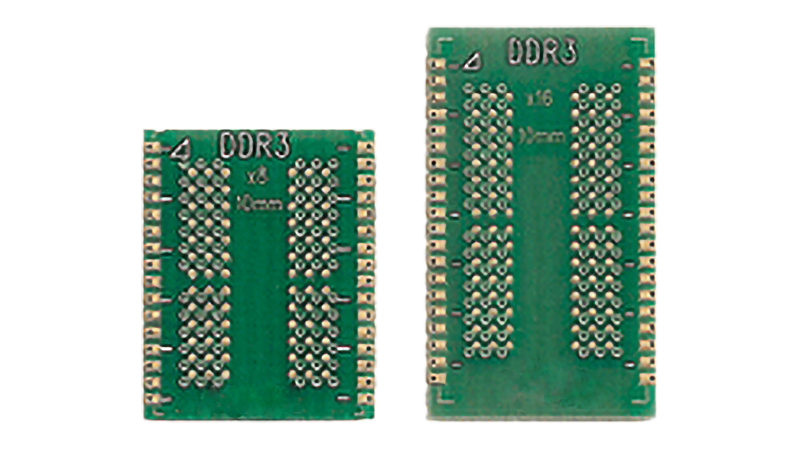
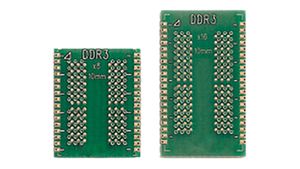
- Provides signal access points for DDR3 DRAM x4, x8 and x16 packages using JEDEC-standard common BGA footprints to the oscilloscope
- 10mm and 11mm BGA probe adapter widths for different spacing requirement between the DRAM placements on the PCB or DIMM
- Buried resistors provide signal isolation and minimize capacitive loading
- Probing compatibility with InfiniiMax probe, which includes E2677A, N5381A, N5425A and N5426A differential solder-in probe heads
- For LPDDR2/3/4 BGA interposer information, visit Keysight Digital BGA Interposer catalog
The Keysight Technologies W2635A and W2636A DDR3 BGA probe adapters provide signal access to the clock, strobe, data, address and command signals to the DDR3 BGA package for making electrical and timing measurements with an Infiniium oscilloscope. With the DDR3 JEDEC specification (JESD79-3A) defined at the DRAM ballout, the BGA probe adapter provides direct signal access to BGA package for true compliance testing.
The W2635A and W2636A DDR3 BGA probe adapters are soldered in between the DRAM and PC board or DIMM raw card where the DRAM would normally be soldered. They are designed with the PCB or DIMM foot print on the bottom side and the DRAM footprint on the top side. The signals from the memory controller chip and DRAM are then passed directly to the top side of the BGA probe adapter where they can be accessed with the oscilloscope probes.

Interested in a W2635A?
Featured Resources


Want help or have questions?
- © Keysight Technologies 2000–2024
- Privacidade
- Mapa do site
- Termos
- Trademark Acknowledgements
- Contate o Webmaster