Confirme o seu país ou área
Por Favor, Confirme
Confirme o seu país para ter acesso a informações sobre preços aplicáveis, ofertas especiais, eventos e contatos.
O que você está procurando?
On-Wafer Measurements
Automated on-wafer measurements for semiconductor device modeling and characterization

Automate On-Wafer Measurements
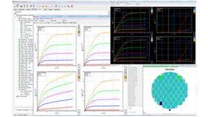
Accurate DC/CV and RF statistical modeling of semiconductor devices requires collecting a significant amount of measured data from different wafers across multiple temperatures.
Keysight provides an automated, turnkey solution for device modeling engineers to achieve more efficient on-wafer measurements. The solution includes the following features.
- Over 50 turnkey measurement drivers fully optimized for speed
- Comprehensive support for industry-standard probers such as Form Factor, MPI, Accretech, TEL, and others
- Integrated Wafer Map support
- Extensive libraries of measurement algorithms
- Python/PEL Programming Environment to enable custom measurements, post-process algorithms, and pass/fail conditions

Accurate, automated on-wafer measurements
On-wafer measurement automation is critical to achieving the throughput and accuracy you need in your production and R&D environments.
Keysight and FormFactor provide all critical building blocks for wafer-level device characterization.
FormFactor’s wafer-level probe station, probes, and calibration tools combined with Keysight’s test instrumentation and measurement and analysis software enable engineers to perform on-wafer DC parametric, IV & CV curves, and calibrated S-parameter measurements on devices at frequencies up to 120 GHz.
Measure Semiconductor's flicker(1/f) noise with wafer mapping
Keysight provides a turnkey solution to measure flicker (1/f) noise and random telegraph noise (RTN). Keysight's Advanced Low-Frequency Noise Analyzer (A-LFNA) enables a closer look at noise in components, individual devices, and integrated circuits, both packaged and at the water level. Thanks to seamless integration with WaferPro Express software, modeling engineers can program and sequence high-speed DC, capacitance, and RF measurements, while automating wafer prober control.

Find the Product That's Right for You

Protect Your Innovation Investment


Featured Resources for On-Wafer Measurements


On-Wafer Measurement FAQ
On-wafer measurement, or wafer-level measurement , is crucial for semiconductor device modeling, process development and specification, process monitoring, component specification, and pilot manufacturing. This process involves the direct measurement of the electrical performance of a device, such as a transistor, diode, capacitor, or integrated circuit, on the wafer before dicing it. Accurate and repeatable on-wafer measurements are essential for understanding the behavior of semiconductor devices under various conditions and ensuring that their performance meets the required specifications.
Device modeling measurements demand higher accuracy than standard production measurements, making them inherently more resource-intensive. Device modeling teams face several key challenges.
Extensive measurement requirements
Production tests may require only single-point spot measurements on process control monitors. Device modeling, on the other hand, requires both swept and spot measurement tests across multiple temperatures (typically three). This process is essential to characterize how a device model changes with temperature accurately. In a standard metal oxide semiconductor (MOS) process, gathering data across a wafer lot at each temperature involves measuring various geometries, capacitance, and diode structures. This process can extend over hours.
Wafer and prober realignment
Temperature variations during measurements lead to the wafer's thermal expansion in all directions (including the z-axis), necessitating frequent realignments of the wafer / prober setup. While sophisticated algorithms using pattern recognition technology might automate this realignment, manual intervention is often necessary at each temperature change.
Challenges at higher frequencies
Characterizing devices at high frequencies often involves measuring scattering parameters (S-parameters), which focus on the frequency and amplitude of waves rather than current and voltage. These measurements, determining the loss and phase change of transmitted and reflected signals, are crucial for accurate characterization. However, they present significant measurement challenges because of the complexities of capturing signal behavior at high frequencies.
Various factors can impact on-wafer measurement results, especially at millimeter-wave frequencies. Understanding and controlling these factors is critical for engineers to ensure accurate device modeling and characterization.
- Calibration method and reference plane choices: Calibration corrects systematic errors in measurement setups. However, the choice of method and reference plane must align with the specific requirements of the frequency range.
- Parasitic circuit elements: Parasitic elements arising from the interconnection between the probe and contact pads (like parasitic capacitance and inductance) can distort the measurements.
- Test environments: The material composition of the wafer chuck used during measurements (whether metallic, ceramic, or another material) can have profound effects on the results.
- Coupling between adjacent neighboring structures: In densely packed device layouts common to modern semiconductor wafers, electromagnetic coupling between adjacent devices or structures can lead to interference that affects measurement accuracy.
- Cross talk between probes: With multiple probes in proximity, often required for complex measurements, electromagnetic cross talk between the probes can occur. This phenomenon occurs when signals from one probe affect the signals of another, contaminating the measurement data with unwanted interference.
Given the time-consuming nature of these measurements — often spanning several hours to days — automating the process becomes paramount.
First, it is crucial for the measurement control software to integrate with the prober's native control software and each instrument involved, automating measurements across temperature.
To maximize efficiency and avoid measuring bad devices, the software should also perform preliminary check tests to assess the die integrity. Based on these initial test results, engineers can make informed decisions on whether to proceed with further measurements, skip faulty devices or dies, or stop the measurement.
Moreover, the ability to monitor measurement results in real time during the execution of the test plan enables immediate detection of any failure conditions and prompt intervention to correct the issues.
Considering the large volumes of data generated by these extensive measurements, efficient data management and analysis capabilities are vital. The software should facilitate the organization, storage, and analysis of data to identify the typical set of devices for modeling extraction.
When deciding between developing custom software or purchasing commercial solutions for R&D device characterization labs, several key factors come into play.
Custom software development using languages like Perl, MATLAB, LabVIEW, C#, or Python gives labs more control over new features, custom drivers, and data handling. However, building mature measurement software from scratch requires a significant investment of time and resources. It can take months to develop a solution that integrates seamlessly with prober and measurement systems. This delay often leads to hidden costs that are not immediately apparent at the outset of the project. These costs can include not only the direct software development and maintenance expenses but also the opportunity cost of delayed project schedules.
Want help or have questions?
- © Keysight Technologies 2000–2024
- Privacidade
- Mapa do site
- Termos
- Trademark Acknowledgements
- Contate o Webmaster