Confirm Your Country or Area
Please Confirm
Confirm your country to access relevant pricing, special offers, events, and contact information.
What are you looking for?
ADS 2017 Product Release

Highlights
ADS 2017 delivers 3D solutions and more for challenging wireless communications design including:
- 3D Layout Viewing, Routing, and Editing
- Multi-Technology 3D Electrothermal Simulation
- 3D Data Visualization with a Python Data Link
- More Powerful 3D EM Simulation with FEM
- 3D Via Designer: Enabling Access to Accurate Via Models
- Automated PCell Construction for Coils and More
- New Option for Hierarchy Management
- Improved Interoperability
- SOA Support for Better Reliability
- Enhanced Circuit Simulation Performance
ADS 2017 delivers new features and capabilities for Signal Integrity (SI) and Power Integrity (PI) design:
- PIPro – DC Electro-Thermal Simulation for Power Delivery Networks
- PIPro - Bill of Materials Optimizer for Decaps and Inductors
- 3D Via Designer: Enabling Access to Accurate Parameterized Differential Via Models
- IBIS Model Usability Improvement and new IBIS Package Model Component
- Significantly Improved Transient and Channel Simulation Speed for Batch Simulations and for use of High-Port Count S-parameters
- Statistical Channel Sim Updated to support PAM4 IBIS-AMI Models
- Substrate Editing in a Table-Based View
Click the links below to watch the:
- Top 10 New Signal Integrity and Power Integrity Features in ADS 2017
- Introduction to PIPro's New Thermal Capability
ADS 2017 Update 1.0 is available for download today (see Important Information about ADS Update Releases).
Description
 With this new release of Advanced Design System (ADS) 2017, Keysight builds upon its industry leading RF/MW circuit simulation software platform with improvements in customer experience (3D Viewer, Quickstart Guide, Python Data Link) and performance (circuit and FEM simulation speed, handling complex layouts, multi-technology support). This together with many other new features help to make the life easier for those who do both RF Front-end module and RFIC silicon design.
3D Layout Viewing, Routing, and Editing
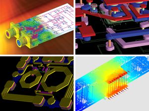
The increased complexity of today’s wireless communications designs demands improved solutions for viewing and editing. This complexity is no match against the new 3D design capabilities in ADS 2017. With these 3D capabilities, it is now possible to visualize and edit a PCB or MMIC/RFIC layout in three dimensions (Figure 1). This provides designers a powerful tool for verifying that designs meet requirements, while also helping them find detrimental mistakes. ADS 2017’s new 3D capabilities also greatly simplify stitching with vias in a multi-layered design, routing in dense areas, and making complex structure selections while preparing for EM simulation.
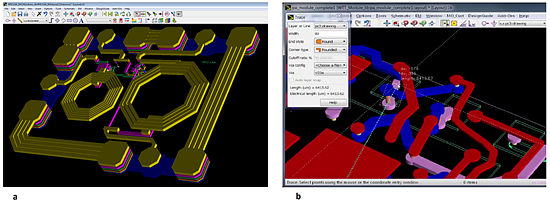
Figure 1. 3D editable views of a) an RFIC layout for an LNA, and b) a PA module PCB now available in ADS 2017.
Multi-Technology 3D Electrothermal Simulation
Designing intricate modern power amplifier (PA) modules requiring high-density layouts or employing advanced semiconductor processes (e.g., GaN and GaAs) can be a tricky proposition. To avoid costly circuit revisions, designers must take a deep look at the thermal performance of the circuit prior to its tape out.
For many years, the ADS Electro-Thermal simulator has provided designers with a full 3D thermal solver that is tightly integrated with the ADS layout environment and circuit simulators. It computes the full system or chip temperature profile, and annotates this information in the circuit simulator for temperature-accurate circuit analysis. ADS 2017 takes these capabilities one step further by allowing multi-technologies to be thermally simulated together.
As an example, consider a PA design that is flip-chipped and encapsulated in a Quad Flat No-Leads (QFN) package. The design includes the die, laminate, copper bumps, and packaging, creating a highly variable thermal resistance profile that is naturally quite difficult to analyze. Figure 2 summarizes the multi-technology substrate setup inside ADS 2017. Figure 3 shows the thermal effects of the building blocks of the entire 3D chip with excellent resolution and accuracy. Included in the thermal analysis are all the design’s structures. With this information, designers can make any necessary edits and subsequently, tape out with a high degree of confidence.
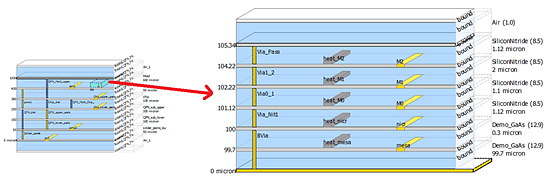
Figure 2. In this substrate setup for a flip-chipped and packaged power amplifier, all the building blocks, including an expanded view of the PA die, are shown in ADS 2017.
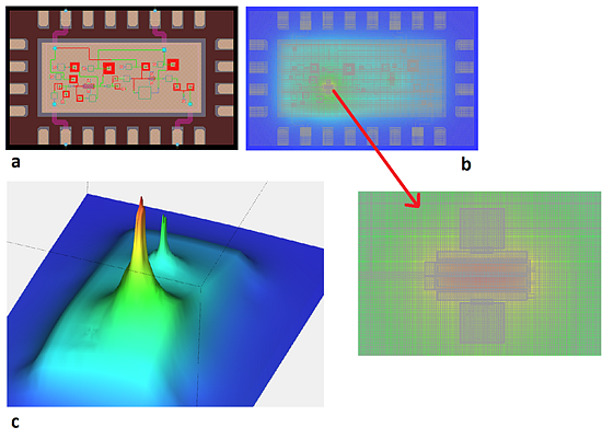
Figure 3. Multi-technology electrothermal simulation can be performed in ADS 2017. Shown here are the a) layout with QFN package, b) 2D thermal profile of the 3D structure, including the die, laminate, copper bumps, and QFN package, and c) 3D thermal profile of the whole chip.
More Powerful 3D EM Simulation with FEM
The 3D Finite Element Method (FEM) engine in ADS is a powerful full-wave EM simulator used to analyze 3D EM effects in the frequency domain. it is especially useful in simulating the EM effects of components such as high-speed and RFIC packages, bond wires, antennas, on-chip and off-chip embedded passives, and PCB interconnects. The FEM engine is fully integrated inside both ADS and Keysight’s 3D modeling and simulation environment, EMPro. Exporting and importing designs to and from the engine is automated, saving time and money, and minimizing errors compared to the manual exporting/importing of designs required with third-party EM simulators. It is estimated that the transfer between the tools alone takes around two hours per simulation. Assuming a single simulation per day, this adds up to a significant time commitment, costing around $50,000 annually! By integrating FEM inside ADS and EMPro, Keysight’s solution saves all that money and the associated frustration.
With the release of ADS 2017 and EMPro 2017, the FEM engine is now more powerful than ever (Figure 4). A smarter mesh creator, adaptive meshing algorithm, use of mixed-order functions, and parallel frequency point solving, allow FEM in ADS 2017 to run 1.5x to 2x faster (on average) than its predecessor (Table 1). In addition, its disk space footprint is reduced by approximately 50 percent. This makes the FEM engine more accessible to RF and microwave designers working to address new and challenging design requirements.
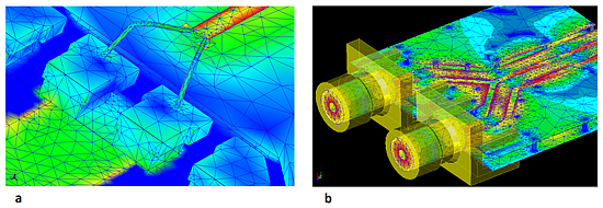
Figure 4. Shown here are FEM-generated EM waves for these 3D structures: a) chip package and bond wires and b) PCB with board interconnects. FEM in ADS 2017 is now 1.5x to 2x faster (on average) and its disk space footprint is reduced by approximately 50 percent from its predecessor.
| Test Case | FEM 2017 Simulation Time |
FEM 2017 Simulation Speedup |
|---|---|---|
| A1 | 0:15:46 | 1.7x |
| A2 | 2:04:05 | 3.8x |
| A3 | 0:00:48 | 1.8x |
| B1 | 1:12:05 | 1.4x |
| B2 | 0:57:19 | 1.8x |
| B3 | 0:32:11 | 3.2x |
| B4 | 0:55:36 |
1.8x |
| C1 | 3:24:53 | 2.6x |
| C2 | 4:51:00 | 1.4x |
| C3 | 0:58:54 | 6.6x |
| D1 | 0:36:07 | 3.8x |
| D2 | 1:46:59 | 6.8x |
| D3 | 0:04:06 | 2.6x |
| D4 | 0:01:58 | 5.8x |
3D Via Designer: Enabling Access to Accurate Via Models
A crucial problem when simulating high-speed signal interconnects is a lack of access to via models that are accurate at high frequencies. To solve this problem, ADS 2017 introduces Via Designer, a tool for creating and modeling PCB vias (single-ended or differential), while giving the designer full control over the via specifics (Figure 5).
Via Designer uses FEM to fully characterize the EM effects of the created model with high-frequency accuracy. It supports parametrized sweeps, enabling fine tuning in the circuit during full-channel simulation. Using this powerful new tool, the uncertainty associated with via design is fully eradicated.
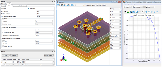
Figure 5. ADS 2017 introduces Via Designer, a tool for creating and modeling PCB vias, shown here with simulation results.
Automated PCell Construction for Coils and More
Abundant and capable simulation options and integration with Keysight’s GoldenGate software—the gold-standard in RFIC simulation—make ADS an excellent platform for starting and completing silicon RFIC designs. ADS 2017 further complements this functionality with the addition of CoilSys, an add-on utility that automates parametrized cell (PCell) construction for spiral inductors, transformers, and transmission lines (Figure 6). The resulting PCells are Design Rule Checking (DRC) clean and ready to be used in an RFIC design. CoilSys eliminates the manual creation of these layout cells, which is often a laborious task; one that does not make efficient use of the RFIC designer’s time.
The layouts created with CoilSys are EM simulated and can be parametrized for component synthesis, as well as for design optimization.
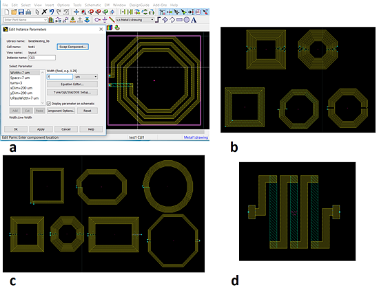
Figure 6. ADS 2017 introudces CoilSys, an add-on utility that automates PCell construction. RFIC designers can create DRC-clean PCells using a) CoilSys for b) single-ended or differential inductors, c) baluns/transformers, and d) solenoids.
New Option for Hierarchy Management
ADS 2017 offers a new option for the creation, change, and control of the design hierarchy using a single graphical user interface. The option, Config View, has its interface illustrated in Figure 8. Unlike older versions of ADS, hierarchy management requires no modification of the design with Config View.
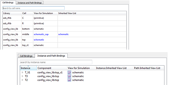
Figure 7. The hierarchy management inside ADS 2017 using the Config View option makes creating, changing, and control design hierarchy so much easier.
A Stronger, More Comprehensive Simulation Platform
Wireless communications system design is never an easy task. It’s even more challenging in today’s fast-paced and dynamic industry. Building on the strong foundation and loyal users ADS has amassed through the years, ADS 2017 delivers new options and functionality that enable it to effectively address existing and emerging challenges facing modern microwave and RF designers. In an environment where even the slightest edge can mean the difference between design success or failure, the powerful and comprehensive new features in ADS 2017 may be just the tool today’s designers need to get ahead.
New for Power Integrity Analysis in PIPro
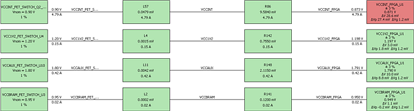
Figure 8. Power Tree results view.
PIPro in ADS 2017 includes a new Power Tree overview plot, generation of detailed analysis reports, and a ‘compare-to’ feature that can quickly show the delta between the results of two simulation analyses. PIPro adds new simulation capability for Electro-Thermal analysis, and a Bill of Materials optimizer for decaps/inductors in the power delivery network.
DC IR Drop Electro-Thermal
Fully-automated, integrated Electrical-Thermal-Electrical iterative simulation
Easily copy existing DC IR Drop simulation setup to new Electro-Thermal simulation
Visualize a list the temperature of planes, pins and vias
Most accurate representation of DC IR Drop results by taking into account local resistivity changes due to heating
Test potential cooling solutions such as increasing the heatsink size, or increasing airflow
Additional Thermal-only simulation, gives the user the ability to perform thermal floor planning
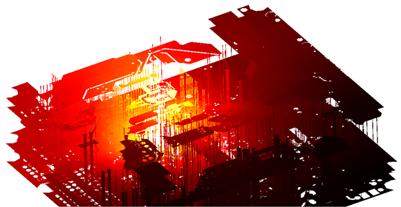
Figure 09. DC IR Drop Electro-Thermal analysis - visualization of temperature.
Bill of Materials Optimization for Decap/Inductors
Reference designs for many ICs provide a comprehensive list of decaps that should be placed on the PDN for best performance and reliability. This doesn't take into account the specific constraints that the designer may have on their PCB (size and layer count). Often there is not enough space around the IC and below the IC, to place all of the decaps, leaving the layout engineer to place the remaining components wherever they fit on the PDN. Decap Optimization in PIPro can take all the decaps as laid out on the board, and search for the optimal solution that meets the desired target impedance profile.
The user can define an optimal solution, by specifying weighted criteria such as:
- # of decaps
- # of unique models
- # of vendors
- Cost
The optimization is fast, by nature of the intelligent algorithms, and the fact that changing decap models does not require a re-computation of the EM solution. The optimization results are presented a list of candidate solutions that meet the target impedance, and are ranked according to the weighted criteria. For each candidate solution, the user can view the PDN Z-impedance vs target impedance, to quickly decide upon the best mix of performance and cost-reduction.
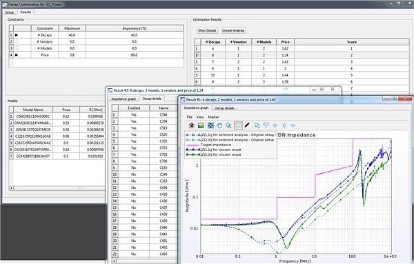
Figure 10. Decap Optimization analysis results.
Learn More
View other ADS Product Versions.
Learn more about Keysight Advanced Design System (ADS)
*The concept of 3D Smith Charts was pioneered by a team at Baylor University led by Dr. Baylis.
- © Keysight Technologies 2000–2024
- Privacidade
- Mapa do site
- Termos
- Trademark Acknowledgements
- Contate o Webmaster