What are you looking for?
Device Characterization and Data Analysis
DC / CV and RF device characterization and modeling require collecting extensive measured data from different wafers over several temperatures. This page explores the essential considerations and requirements for effective device characterization, focusing on DC/CV test cells, RF test cells, and special measurements for low-frequency noises (LFNs).
Key components in DC / CV test cells
A standard DC / CV measurement test cell includes the following components:
- A semi-automated prober with thermal chuck.
- A DC Analyzer such as the Keysight B1500A semiconductor parameter analyzer or the Keysight E5270B Precision IV Analyzer.
- A switch matrix such as the Keysight B2200 fA leakage switch mainframe if a probe card is used.
The Keysight Parametric Test Solutions offer an advanced alternative to benchtop instruments for device modeling teams aiming for higher throughput.
Key components in RF test cells
To ensure accurate RF device characterization, an RF test cell requires the following elements:
- A semi-automated prober with a thermal chuck.
- A DC Analyzer or power supply.
- A Keysight Network Analyzer such as the Keysight PNA-X or PNA.
- Bias networks at each port to combine DC and RF signals.
The frequency range of these RF test cells may range from a few tens of MHz to 110GHz or higher.
Noise measurements
In addition to standard DC and RF test cell requirements, special measurement systems such as a 1/f noise analyzer are necessary for accurately analyzing low-frequency noise (LFN) and extracting critical parameters. Measured data for flicker and Random Telegraph Signal (RTS) noise are vital to monitoring process reliability in advanced CMOS technologies.
Learn about the E4727B Advanced Low-Frequency Noise Analyzer (A-LFNA).
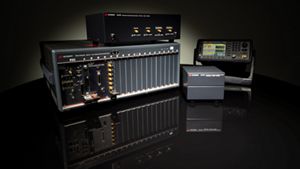

Figure 1. Advanced Low-Frequency Noise Analyzer enables fast, accurate, and repeatable low-frequency noise (LFN) measurements on numerous device types.
Two key requirements
There are two fundamental requirements when conducting measurements for device characterization and modeling.
Accuracy
This generally depends on the instrument performance and the quality and characteristics of the system components (e.g., cabling, connectors, bias networks, prober and probes, etc.). Effective RF calibration and de-embedding play a key role in the measurement accuracy of RF measurements.
Efficiency
The instrument speed, the measurement software drivers, and test algorithms play significant roles in accelerating time-to-results.
One of the major challenges is automated measurements over temperature. Due to wafer and hardware expansion (or contraction), the wafer mapping software may lose control of the alignment in the X and Y directions. Chuck or probe card expansion can result in major contact problems or damage in the vertical (Z) direction. Pattern recognition technology is critical to overcome these problems and enable automated wafer test measurements over temperature.
Automated wafer-level measurements
Keysight’s WaferPro software enables device modeling engineers to automate wafer-level measurements for efficient device characterization. The platform combines the ability to drive probers, switching matrixes, and thermal chucks according to a predefined wafer map, with the ability to run complex DC / CV and RF measurements using a variety of instruments—from parametric testers to single box instruments.
Furthermore, the analysis of measured data is crucial for extracting Electrical Test (ET) data, such as threshold voltage (Vth,), maximum drain current (Idmax,), or fT.

Figure 2. IC-CAP Wafer Professional Measurement.
Free Trials
Additional Resources
Explore our additional resources to learn how Keysight can help you address measurement challenges and elevate device characterization and data analysis.
Want help or have questions?