Confirm Your Country or Area
Please Confirm
Confirm your country to access relevant pricing, special offers, events, and contact information.
What are you looking for?
N2114A DDR4 BGA Interposers, DDR4 DRAM x4/x8 packages
Test, debug, and characterize your DDR4 designs with direct signal access to the BGA package
Starting from
HIGHLIGHTS
- Provides signal access points for DDR4 DRAM x4/x8 packages using JEDEC-standard common BGA footprints to the oscilloscope
- Perimeter solder-down test points can be used with Logic Analyzer flying leads or Oscilloscope solder-down probe tips to access signals
- Effective bandwidth may be extended with InfiniiSim Waveform Transformation software
- Measurement timing skews reduced by matched trace lengths from DDR4 balls to test points
- Probing compatibility with InfiniiMax probe, which includes E2677A, N5381A, and N5425A/N5426A differential solder-in probe heads
- S-parameter models are available for use with InfiniiSim for de-embedding purposes
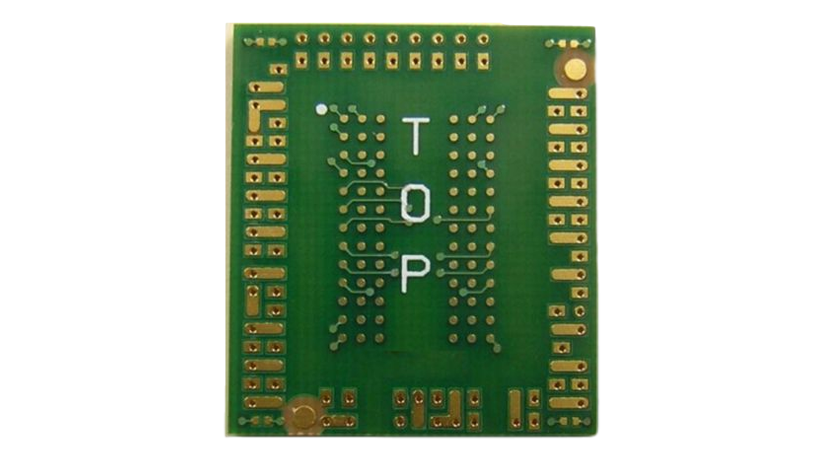
The N2114A DDR4 BGA interposers provide signal access to the clock, strobe, data, address and command signals to the DDR4 BGA package for making electrical and timing measurements with an Infiniium oscilloscope. With the DDR4 JEDEC specification defined at the DRAM ballout, the BGA probe adapter provides direct signal access to BGA package for true compliance testing.
The N2114A DDR4 BGA Interposers are soldered in between the DRAM and PC board or DIMM raw card where the DRAM would normally be soldered. They are designed with the PCB or DIMM foot print on the bottom side and the DRAM footprint on the top side. The signals from the memory controller chip and DRAM are then passed directly to the top side of the BGA probe adapter where they can be accessed with the oscilloscope probes.
Interested in a N2114A?
Featured Resources for N2114A DDR4 BGA Interposers, DDR4 DRAM x4/x8 Packages


Want help or have questions?