What are you looking for?
PathWave Advanced Design System (ADS) 2020 Product Release
Highlights
PathWave Advanced Design System (ADS) 2020 delivers new features and capabilities for:
- RF & Microwave Design
- Signal Integrity and Power Integrity Design
- Power Electronics Design
PathWave Advanced Design System (ADS) 2020 is available now!
Description
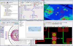
![]() PathWave Advanced Design System (ADS) 2020 is the next major step in delivering new capabilities, new technologies and more improvements to further improve design productivity and efficiency.
PathWave Advanced Design System (ADS) 2020 is the next major step in delivering new capabilities, new technologies and more improvements to further improve design productivity and efficiency.
Figure 1. PathWave Advanced Design System (ADS) 2020.
RF & Microwave Design
What's driving the need for change in RF & Microwave design?
- Design Complexity: 20+ ICs, more elaborate interconnect & packaging dramatically increases the need to productively design & analyze multi-chip RF IC/Modules for electro-magnetic, thermal effects on design performance
- 5G Design Challenges: higher frequencies (6GHz & 28GHz+) and broadband modulation, greater amounts of data (simulation & measured) to analyze
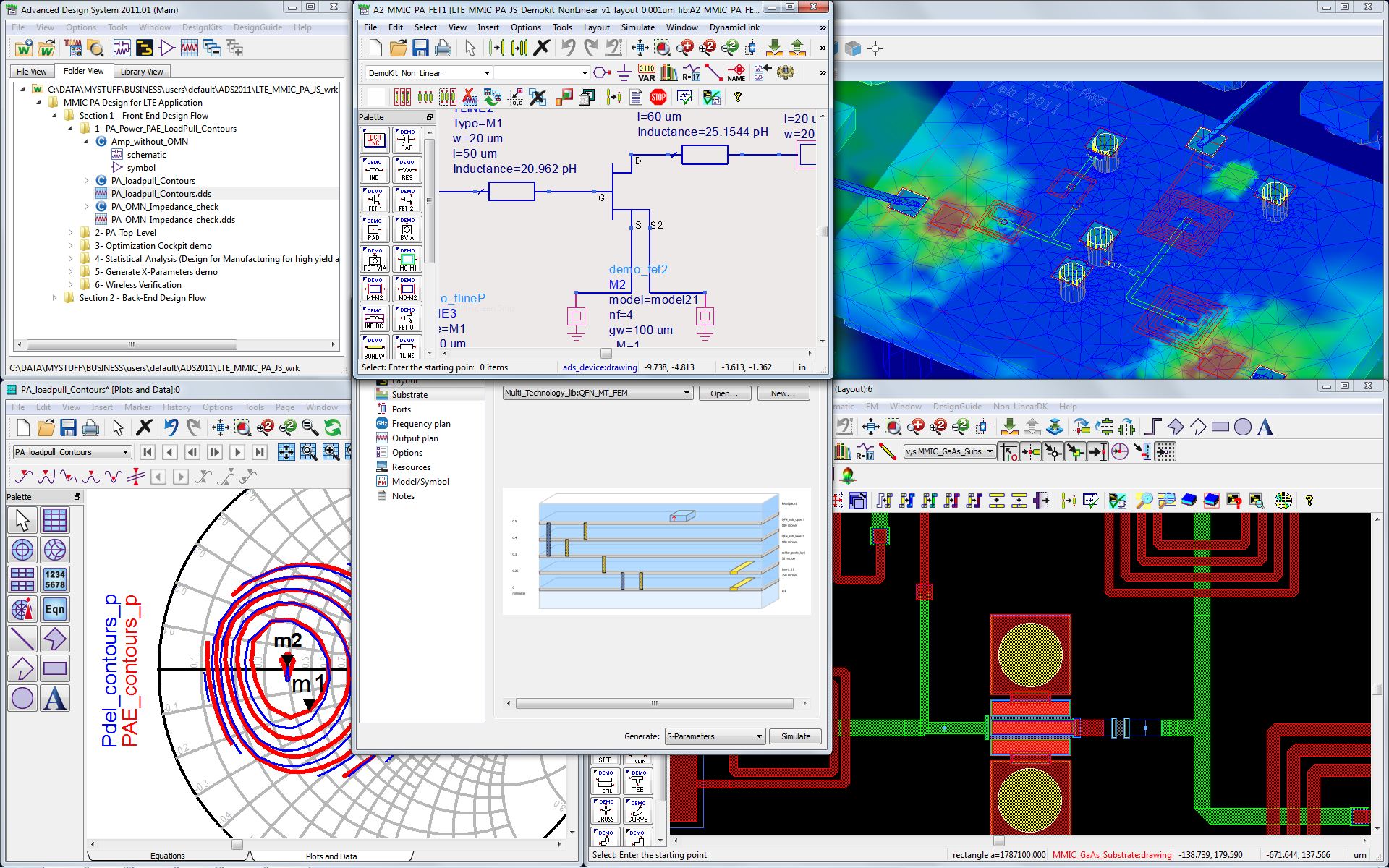
RFPro & EM Simulation
- RFPro: the 1st EM platform for circuit and module designers
- Modern 3D user interface
- Automatic settings
- No modification to the original layout
- Improved Momentum and FEM solvers
- RFPro Net extraction
- RFPro Multi-Technology support in ADS
Electro-Thermal Simulation
- Transient/CE Performance
- Allow mismatched hierarchies
Wireless Verification
- 5G New Radio Verification Test Bench
ADS Platform & Data Visualization
In ADS 2019, we introduced several workspace management features. In ADS 2020, we made it better by adding an explain feature to enable users to explicitly understand independencies between objects inside a workspace and even open the design and highlight the specific location of the dependency. We also added the capability to trace connections between schematics, datasets and Data Displays.
We've also improved Data Display in Several Ways:
- Capacity: Memory mapping for faster reading of large datasets and faster zooming and panning on plots
- Usability: Expression manager allows users to view, select, and modify all their DDS equations in a single spreadsheet form. Find, replace copy and paste capabilities make it easier to build or modify data display templates, and netlist (text) export options for equations allow DDS equations to easily be converted into Schematic-based measurement equations so they can be saved directly in a dataset.
- Finding Problems: Right Click and Find Equation Menu enables users to identify other equations which the current equations reference, so problems can be easily identified and fixed.
Physical Design
In ADS 2019 Update 1.0, we introduced padstacks, which are package level layout building blocks. These can be used to build stackable, constrainable PCB VIAs which can also have custom keepouts and clearances. In ADS 2020, we've added PCB VIAs to the references database, so workspace management tools can also identify interdependency. We also added the ability for padstacks on Smart Mount Multi-technology components to have their properties transfer to higher level technologies. For example, if an IC with padstacks is mounted on a PCB, a ground plane on the PCB would honor the clearance of the IC level pad.
Added a Constraints Manager for package design infrastructure. This consists of a GUI and a single file for a library that defines all of the design constraints used for interactive features such as planes and avoidance routing. Previously, these were stored in multiple places, now they are in a single place. Constraints are both easy to define and powerful; for example, a user can specify that a ground plane has a different clearance for Power and Ground nets.
Verification
- PDK Validator: improving PDK quality, efficiency & DRC/LVS support
Signal Integrity and Power Integrity Design
Memory Designer
Memory Designer provides predictive, productive, and insightful workflow for memory design and test.
- Automated wiring connections, utilizing Signal IDs found in the layout design
- DDR Bus simulator to characterize signal integrity, capturing margin-to-mask tests for ultra-low BERs
- New Memory Probe to set up measurements by group, with intelligent selection of signal references
- Automated DDR4 Compliance Test suite and report generation, utilizing Keysight’s industry recognized DDR4 measurement science
Channel Simulation
ADS Channel simulation now connects to FlexDCA application and supports Channel Operating Margin (COM) and MIPI C-PHY and more.
- The standard simulation tool for MIPI physical layers (D-PHY, M-PHY, C-PHY, A-PHY). MIPI physical layers support various mobile and automotive device applications
- Support for Channel Operating Margin (COM) enables designers to explore physical design budget (choices) between loss, reflection ISI, crosstalk, and device specifications
- Connection to Keysight sampling scope software FlexDCA to unlock all built-in comprehensive PAM4 analysis for electrical and optical links
PIPro
PIPro provides different discrete switching VRM models to accurately capture the DC current density.
- Support for sense lines and discrete VRM models (Buck, Boost, Inverting) to accurately predict DC IR drop
- Advanced algorithm to speed up simulation and decrease required memory to run
- Flexibility to import user-defined circuits in PIPro EM simulation
SIPro
- Supports intuitive DDR EM extraction setup and speeds simulation time with additional parallelization
Via Designer
- Now supports DDR multi-drop vias, stacked and staggered micro-vias
Power Electronics Design
The new W2376EP/ET PEPro, Momentum, FEM Element makes post-layout analysis of switched-mode power supplies as easy a pre-layout analysis.
Learn More
View other ADS Product Versions.
Return to Keysight Advanced Design System (ADS)