Toggle Menu
What are you looking for?
Suggested searches
No product matches found - System Exception
Matched content
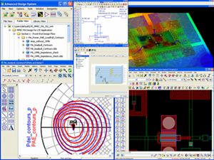
ADS 2014.01 Product Release

Highlights
Advanced Design System (ADS) 2014 includes the following new products and improved capabilities:
- Automatic EM/Circuit Simulation Setup & Partitioning
- New Physical LVS with Device Recognition
- New Wireless Verification Test Benches (LTE-A, LTE, 802.11ac)
- Improved Layout Interconnect Design & Editing
- Controlled Impedance Line Designer
- Silicon RFIC Schematic Interoperability with Virtuoso
- ADS Board Link – Next Generation PCB Integration Solution
- Simulation Support for DynaFET model
Description
ADS 2014 is the next major step in delivering new capabilities, new technologies and more improvements to further realize a long-term vision to improving design productivity and efficiency through design flow integration.
Automatic EM/Circuit Simulation Setup & Partitioning
- ADS’s popular Layout Lookalike capability lets the designer set up a circuit/EM co-simulation where the schematic models (e.g., SMT parts or active IC devices) are connected to a “lookalike” representation of the layout.
- For cases where the device-count grows to dozens or even hundreds—ADS 2014 now offers a new automated EM/Circuit Simulation Setup capability resulting in substantial time savings and elimination of manual errors.

W2320EP/ET Advanced Layout (Physical LVS with Device Recognition)
- Industry standard methodology for IC verification and foundry signoff.
- Includes mode based on p-cells, without the need for a rules file.
- P-cell mode works with module, multi-technology designs and pin nets for a robust module level LVS solution.
New Wireless Verification Test Benches (VTB)
- Wireless VTBs provide circuit design verification solutions for the newest and most challenging multi-band, wide-bandwidth standards (LTE, LTE-A and 802.11ac) with a dramatically simplified user interface.
- New VTBs and the underlying simulation technology are based on the SystemVue dataflow simulation technology and also allow system architects to develop custom VTBs for use by circuit designers in ADS.
- Simplified VTBs offered at a significantly lower cost than Ptolemy-based Wireless Libraries.
Improved Layout Interconnect Design & Editing
- Vias can now be used as layout interconnect objects, so they can be used more efficiently in routing and automatically resized during trace width insertion.
- New planes allow designers to create a layer of copper to carry a particular signal on a printed circuit board (PCB).

W2307EP/ET Controlled Impedance Line Designer
- Create a pre-layout channel in an end-to-end ADS Channel Simulator schematic.
- Optimize the metrics that matter:
- Eye Diagram parameters including mitigation
- Bode plots of the channel impairment
- Design the stack up and line geometry of the controlled impedance lines.
- Determine the parameters that you feed into the Constraint Manager of the auto-router in your enterprise PCB tool.

Combining the line type with a statistical eye Channel Simulation enables you use metrics that matter -- such as post-equaliztion eye opening height and width -- to optimize your controlled impedance lines.
W2319EP/ET Silicon RFIC Schematic Interoperability with Virtuoso
- Bi-directional schematic interoperability w/Virtuoso.
- Bring Virtuoso schematics in ADS and simulate RF performance.
- Front-end design in ADS and layout implementation in Virtuoso.

ADS Board Link (ABL) – Next Generation PCB Integration Solution
- Bi-directional interface for layouts, schematics and libraries between ADS and enterprise PCB tools to be imported into ADS.
- Supports import and export of libraries and technology information (e.g., units, resolution, layers, purposes, and substrates), as well as design data.
- Enables RF schematic and layout designs started in ADS to be easily transferred to the enterprise PCB environment for integration into a larger design for floor planning; modified to accommodate physical design constraints; and then returned to ADS for verification.
- Enterprise PCB layout designs can be imported into ADS via ABL to perform post-layout EM analysis in ADS with little to no need for layout pre-processing before EM simulation.
- ABL design transfer between tools is high-fidelity and preserves all data and original objects.
- Architected to have significantly improved speed and capacity.
Simulation Support for DynaFET Model
- Keysight’s DynaFET Model is an advanced compact model of III-V FETs (GaAs and GaN) including electro-thermal and trapping effects.
- Modeling engineers can automatically extract DynaFET models in IC-CAP.
View other ADS Product Versions.