The increased data rates of today’s high-speed Input/Output (I/O) buses make maintaining transmission channel signal quality all the more challenging. One reason for the challenge is the parasitic effects that result from bus interconnects. Over the past decade, data rates for electrical interconnects have experienced a dramatic increase—from 1 Gbps to 25 Gbps and beyond—to meet the ever increasing demand for more I/O bandwidth from modern networking applications and high-capacity storage.
Enter the Serializer/De-serializer (SerDes), a high-speed serial data link used in ICs to serialize parallel data and transfer it at a much faster rate. Today, Gigahertz SERDES is a leading inter-chip and inter-board data transmission technique for high-end computing devices. PCI Express (PCIe) is a high-speed serial interconnect protocol conceived as a way to overcome many of the limitations in conventional parallel buses, address ever increasing bandwidth requirements and provide much greater performance. It does so by providing a scalable, point-to-point serial connection between chips, while maintaining compatibility with conventional PCI at the software layer. While this bodes well for designers, it also creates a host of challenges, which make signal integrity analysis and compliance testing absolutely essential to ensuring high signal quality.
The Challenge: PCIe 3.0 Interface
PCIe is a standard maintained and developed by the PCI Special Interest Group (PCI-SIG), a community of companies responsible for developing and maintaining the standardized approach to peripheral component I/O data transfers. The third-generation of the PCIe standard, PCI Express Gen3 (PCIe Gen3), specifies a high-speed differential I/O interconnect that runs at 8.0 Gbps. It is widely used in computers and servers.
Figure 1 shows a typical PCIe Gen3 link. In general, the channel may either be short and straightforward, with only a few inches of interconnect between the driver and receiver, or long and complicated. The PCIe 3.0 channel can consist of anywhere from one to 32 lanes. Connectors for multiple widths—x1, x4, x8, x12, x16, and x32, where x represents the lane—are defined by the PCIe standard.

Figure 1. A typical 8-lane PCIe Gen3 link.
The challenge here is that PCIe, using high-speed 8-Gbps serial links, can suffer from a large array of physical phenomena. Such phenomenon might include crosstalk, impedance discontinuities resulting in reflections that cause jitter, Intersymbol Interference (ISI), and mode conversion due to unbalanced transmission lines—all of which can lead to excessive electromagnetic interference (EMI) emissions in large systems.
Solving The Challenge
Addressing this challenge demands a PCIe interface simulation methodology. Simulation is performed to ensure the interface specifications are met, including the eye characteristics, and that the Bit Error Rate (BER) is less than a specified maximum.
With serial channels moving to high data rates, a SI simulation method based on IBIS-AMI models is used to account for different channel parameters. IBIS-AMI is a modeling standard for SerDes Physical Layers (PHYs) that is part of the IBIS 5.0 specification. It enables fast, accurate, statistically significant circuit simulation of multi-gigabit serial interfaces.
In general, a time-domain transient simulation utilizing IBIS-AMI 5.0 transmitter and receiver models can be combined with lossy channel parameters to produce eye diagrams at the receiver end. The results can then be compared with the received Eye Mask, as per the PCIe 3.0 requirement. If the simulated eye is within the eye opening specification for amplitude and jitter, then a better-than-specified BER, usually 10^12-10^17, is achieved. The simulation is used for SI analysis and compliance testing to optimize PCIe Gen3 channel performance to the PCI-SIG specifications.
In particular, the simulation methodologies used for the PCIe interface are:
Channel Simulation
The analysis approach presented here involves transient simulation, whose length is determined by the amount of channel loss and the strength of reflections. The PCIe simulations are run at 8 Gbps (UI=125 ps) with IBIS-AMI models at the transmitter (Tx) and (Rx), including jitter at the Tx and with a channel length of 6 inches. At 8 Gbps; however, with interconnect of significant length, the decision-feedback equalizer (DFE) and feed-forward equalizer (FFE), the IBIS specification is no longer sufficient to represent the Tx and Rx circuits. To overcome this problem, an extension to IBIS, the IBIS-AMI (Algorithmic Modeling Interface), was developed.
Jitters
In serial communication systems, the clock is embedded along with the transmitted data, and the Clock Data Recovery (CDR) circuit is used to recover the clock at the receiver side. Latching the correct data depends strongly on the alignment between data and clock. Jitter plays an important role in the number of bit errors and can be classified as Random Jitter (RJ) and Deterministic Jitter (DJ). To simulate an accurate estimate of the BER, both of these jitter elements must be included in simulation.
Equalization
The PCIe 3.0 specification includes a provision for performing equalization at the transmitter and/or at the receiver. This is done to mitigate the effect of ISI and hence, minimize BER. In equalization, the signal is passed through a filter with a frequency response equal to the inverse frequency response of the channel. A high gain is applied to counter signal attenuation at higher frequencies. In other words, equalization is an adaptive filter with coefficients determined on runtime, depending on the physical channel (Figure 2).

Figure 2. PCIe 3.0 equalization at the transmitter and receiver.
De-Emphasis and Pre-Shoot
PCIe uses transmit de-emphasis to compensate for high-frequency channel losses. A de-emphasized waveform is defined in terms of the voltage levels Va (de-emphasis) and Vb (flat level). Figure 3 shows the resultant output signal when a binary input stream is applied to a 3-tap FIR filter. Note that the output takes a different value just before and after polarity inversion of the input bit stream. Corresponding to these events, the PCIe 3.0 specification defines new terminologies as explained in Table 1. Voltages Va, Vb, Vc, and Vd correspond to de-emphasis, flat level, pre-shoot, and maximum boost events, respectively.


Figure 3. De-emphasis and pre-shoot.
|
PCIe 3.0 Term |
Corresponding Condition on Input signal |
|---|---|
|
De-emphasis (Va) |
A boost appears just after the polarity inversion |
|
Flat Level (Vb) |
A constant voltage will appear when bits of the same polarity are being transmitted |
|
Pre-Shoot (Vc) |
A boost appears just before the polarity inversion |
|
Maximum Boost (Vd) |
A major boost appears when there is polarity inversion only for one bit interval |
Table 1. Different equalization terminologies.
PCIe Signal Integrity Analysis
To perform SI analysis, the PCIe connector, eight-lane data bus, and package are first simulated using an electromagnetic (EM) solver. S-parameter data is then extracted. From this data, important factors from a SI point of view are analyzed, including: impedance matching, reflection, attenuation, impedance mismatch, propagation delay, crosstalk, and the alignment shapes of the connectors. Next, all of this data is re-combined and a Pseudo-Random Bit Sequence (PRBS) is generated at a bit rate of 8 Gbps.
For the purposes of this article, the high-speed digital (HSD) board used in the analysis is a 12-layer, high-speed FPGA digital board. The noise in the channel network mainly affects the system’s jitter performance. This causes degradation in signal quality. For horizontal and vertical transitions, like wire bonds, via array, and the solder balls of the package and printed circuit board, 3D models were generated for use in the SI and power integrity (PI) simulations. EM simulated data is extracted using SIPro for the PCIe 3.0 eight-lane data bus.
The result of the transient analysis with PRBS random data input for the complete channel is shown in Figure 4. The channel combines the EM extracted data of the connector, eight-lane channel and chip package in Advanced Design System (ADS) software. From the eye diagram, it can be seen that the signal degrades over a long transmission path and due to the connectors. The input signal is PRBS-11 serial data at 8 Gbps.

Figure 4. Transient simulation setup and result for the complete Channel.
PCIe Compliance Testing
Compliance is necessary to ensure products are interoperable. It validates that the PCIe channel is compliant with the PCIe specification. Different compliance test parameters are listed in Table 2.
|
Signal |
PCIe Compliance Testing |
|
Transmitter electrical |
TX Signal Quality Test TX Preset Test |
|
Receiver electrical |
Receiver Jitter Tolerance Test |
|
TX/RX Link equalization |
Transmitter initial TX Link EQ Test TX and RX Link Equalization Test |
Table 2. Different compliance test parameters from the PCIe specification.
Transmitter Electrical – Tx Signal Integrity
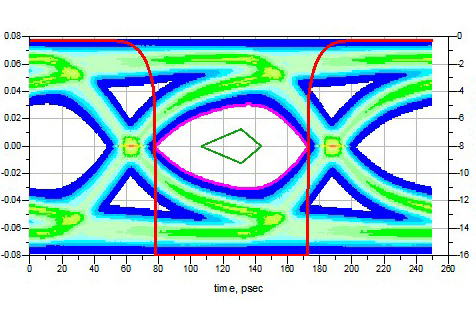
To fully characterize a PCIe transmitter, Unit Interval (UI) time, voltages, eye mask, jitter, idle timing, and lane skew are measured based on the PCI-SIG specification. Most specifications are required to be measured over 250 consecutive UIs. For accurate measurements, a direct connection from the transmitter’s Tx output to its’ inputs should be used. Doing so, ensures the lowest noise measurement. Figure 5 shows the eye and jitter measurement on a transmitter transition bit.

Figure 5. PCIe 3.0 Tx Simulation: eye diagram and waveform.
Receiver Electrical – Equalization
Receivers must be tested for sensitivity and tolerance to jitter. The testing methodology is to provide a stimulus to the Rx input of a device and monitor the response from the device via the Tx pins. The measured eye is combined with the eye mask for compliance test.
As shown in Figure 6, without any equalization, the eye is closed. However, after applying Rx equalization, the eye is open and meets the PCIe specification. The idea behind equalization is to use the voltage levels of the other bits to correct the voltage level of the current bit. Due to the ISI from the frequency-dependent loss of the channel, the eye of the received signals is totally closed, and the clock and data cannot be recovered from the severely distorted signals. After the Decision Feedback Equalization (DFE) equalizer, the eye of the equalized signals is opened and the vertical eye opening at the data center is around 368 mV. This value is large enough for the decision circuit to recover the digital data at an acceptable BER.
|
|
|


Figure 6. Eye diagram (a) without Equalization (b) Feed-Forward Equalization (FFE).
Tx Equalization Setting and Preset Test
The PCIe 3.0 specification specifies a compliance pattern with 10 presets. Once in compliance mode, bursts of a 100-MHz clock can be used to cycle through various settings of compliance patterns to perform jitter, voltage and timing measurements. Compliance test ensures that the Device-Under-Test (DUT) can generate all presets and equalization levels to meet specification requirements. Figure 7 shows the waveforms for all preset values.

Figure 7. Waveforms for different preset values.
Conclusion
Ensuring the high signal quality of PCIe Gen3 serial channels is critical to allowing these high-speed serial interfaces to deliver on their promise of greater performance. Signal integrity analysis and compliance testing are vital tools to accomplishing that goal, as is employing a methodology that relies on IBIS-AMI models. Using these tools and the approach detailed in this article, engineers now have a straightforward and accurate means of optimizing channel performance as per the PCIe-SIG specifications.
References
- K.S. Oh and X.C. Yuan, High-Speed Signaling: Jitter Modeling, Analysis, and Budgeting, Prentice Hall, 2012.
- A.K. Pandey, "Power-aware signal integrity analysis of DDR4 data bus in onboard memory module," Signal and Power Integrity (SPI), 2016 IEEE 20th Workshop on, Turin, 2016, pp. 1-4.