Emerging 100 Gigabit Ethernet and 400 Gigabit Ethernet requirements for communication networks have put increasing demands on Internet infrastructure. New methods of design, validation, and troubleshooting to optimize high speed digital channels are being employed in the R&D laboratory. This article discusses new concepts for serial link design and analysis as applied to physical layer test and measurement techniques. Novel test fixtures and signal integrity software tools will be discussed in real world applications in the form of design case studies.
INTRODUCTION
Today’s internet has touched the lives of many people in ways that were hard to imagine ten years ago. Mobile devices in every pocket push the demand of bandwidth to ever increasing levels, challenging the best engineering minds in the world. Modern internet infrastructure has evolved to support faster data transfer between system components by using bigger pipes and novel modulation schemes to exploit every efficiency method conceivable.
The basic goal of the signal integrity engineer has remained the same: designing the most pristine physical layer that exhibits minimal loss within the channel and maximizes the signal-to-noise ratio at the receiver. This can be achieved in multitude of ways by utilizing sophisticated pre-emphasis and equalization techniques, but the challenge always seems to boil down to optimize the raw unadulterated channel between the transmitter and receiver. This article discusses some new concepts around measurements and simulation of the physical layer that can open the eye diagram at the end of the channel using fundamental building blocks of scattering parameters.
USING S-PARAMETERS TO CHARACTERIZE MODERN SERIAL LINK SYSTEMS
When characterizing a prototype channel within the physical layer of any interconnect such as a backplane, printed circuit board or cable, there are traditional ways of looking at performance data that indicates the quality of the transmitting channel. While there are traditional analysis methods for judging the signal integrity quality including step response, scattering parameters, and eye diagrams, there are many other tools that can be utilized including channel simulation and sophisticated measurements yielding new figures of merit that more accurately assess the real-world performance.
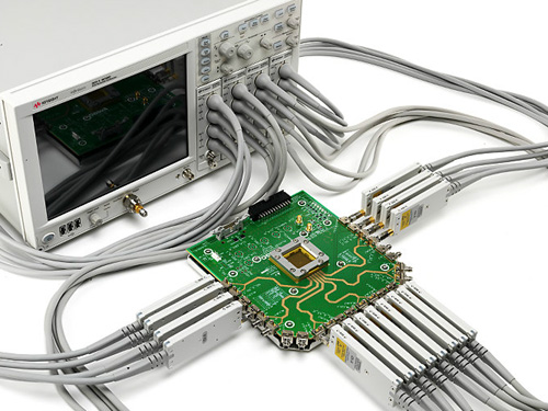
The most popular stimulus-response type test equipment used for this passive interconnect measurement is either the Time Domain Reflectometer (TDR) or the Vector Network Analyzer (VNA). Once the physical layer information is gathered from either instrument, then the data can then be imported to specialist software tools to further analyze multiple domains including time, frequency, reflections, transmissions, single-ended, and differential. These methods are well known in most signal integrity labs today and the test instruments that make these measurements are shown in Figure 1.
There exist some new and interesting options for interconnect analysis. These trending methodologies include single pulse response, Channel Operating Margin (COM), Pulse Amplitude Modulation with 4 levels (PAM4) and multiport mode conversion analysis. The daily routine of the electrical engineer today includes exploring new and novel ways to solve problems by gaining new insight. Many times, this new insight comes from visualizing data in a slightly different way than normal. The link from insight to solution working with high speed digital design can be expedited using various tools known by industry experts with experience in signal integrity problem solving. In many cases, the individual application can be grouped into a general type of problem that has already been solved.

Fig. 1. Typical high speed digital interconnect applications require specialized stimulus-response test equipment such as the Time Domain Reflectometer (TDR) or the Vector Network Analyzer (VNA).
THE CARE AND FEEDING FOR S-PARAMETERS
Traditional microwave applications consist of narrow band modulated systems without time domain requirements such as eye diagrams. Modern serial link characterization places incredible demands on the requirements of measured S-parameters and on the quality of the test fixtures.
For example, it is not difficult to make clean coaxial measurements using a modern VNA with supported electronic NIST traceable calibration. However, very often, test fixtures need to be inserted between an instrument’s coaxial interface and a planar transmission system such as microstrip or stripline. Launching onto the test vehicle is difficult and represents a major challenge for good signal integrity. Therefore, the quality of measured S-parameters of the Device Under Test (DUT) can vary widely, so an IEEE standard, PG370 TG1, 2, and 3 are presently being developed to assist with checking and validating the quality of S-parameters.

Fig. 2. Standard S-parameter measurements are limited by bandwidth having a start frequency, stop frequency and step size (delta f).
The history of S-parameter started even before the publication of Kurokawa’s important paper on “Power Waves and the Scattering Matrix” [1]. It is no question that Kurokawa’s theoretical discussion on the physical meaning of normalized power waves and scattering parameter helped advance the understanding of microwave engineering.
However, the introduction of network analyzer and the touchstone format for measuring and storing the S-parameters aided the spread of S-parameters as well. Nowadays, S-parameters are not only a prevailing behavioral model used in the microwave community; it is also a standard format for describing any interconnect.
Despite of its theoretical completeness in the microwave industry, S-parameters do have their practical limitations in signal integrity applications such as limited bandwidth (as shown in Figure 2). Because signal integrity engineers focus on both the frequency and the time domain, it is not enough to only have a frequency behavioral model of the interconnect. In the following, we will show how the limited bandwidth of S-parameters affects the quality of the time domain model of the interconnect.

Fig. 3. Kramers-Kronig relationship for causal systems.
First, band-limited S-parameters can potentially violate the causal system requirements. Since causal systems satisfy the Kramers-Kronig (K-K) relationship [2], there are strict qualifications for a system to be causal. The qualifications are:
- The real and imaginary components of the frequency response (e.g. S-parameter matrix entries) are interdependent and related by the Hilbert transform.
- The K-K integration relationship, shown in Figure 3, to be satisfied over all frequencies.
Given the stringent requirements, the truncated S-parameter measurement of a causal system generally violates the K-K relationship and leads to non-causal response [3].
In addition to the causality violation, there is also passivity constraint on S-parameter of passive elements. Specifically, a passive system does not generate energy; the definition of passivity for S-parameter at each frequency stipulates that all singular values of scattering matrix are unitary bounded [4]. In practice, any approach to passivity correction requires considerable attention. As Figure 3 suggests, S-parameter manipulation in the frequency domain may violate causality.
Aside from causality and passivity, for digital application in the multi-giga bit regime, another consideration is the bandwidth of measured S-parameter data. It is shown to adequately predict the response at the receiver, the bandwidth of the S-parameter model of the interconnect needs to be at least 60% of the inverse of the driver’s 20-80 rise time [5].
Once we have confidence in the S-parameter quality, the frequency-domain S-parameter model needs to undergo transform algorithms to obtain the time-domain received data pattern. Since the impulse response of a system characterizes the system completely, one facilitates the generation of received pattern by first converting frequency-domain S-parameters to impulse response, and computing output waveforms using time-domain convolution [3]. Once the passivity and causality of S-parameter data is verified, there are many approaches to convert the causal, passive S-parameters into the time domain; one of the obvious approaches is the inverse discrete Fourier transform.
Although the inverse discrete Fourier transform provides a valid conversion method from frequency domain S-parameter data to time domain impulse response, the finite frequency limit of the inverse transform introduces non-causality in the time domain waveform such as Gibbs ripples. Although it is possible to apply a filter to smooth out the abrupt truncation of frequency components and reduce the ripples [6], the applied filters themselves can often be non-causal.
It is not a trivial task to produce a causal and passive impulse response from band-limited S-parameters for time domain convolution analysis. Thus, computing the received time domain waveform demands care in the algorithm and consideration of physicality of system under examination. Nevertheless, given a causal and passive impulse response that accurately characterizes the interconnect, one can compute the received signal by performing a time domain convolution of the impulse response with the transmitted signal.
To learn most about the interconnect under test, a special signal pattern is transmitted. Pseudo-Random Binary Sequence (PRBS) is a binary sequence that, while generated by deterministic algorithm, exhibits statistical behavior like a truly-random sequence. With PRBS, one tests all the possible transitions of the signal levels at a given pattern length.
Having the PRBS pattern as the transmitted signal and the impulse response of the interconnect, the process of discrete convolution produces the received pattern. As shown in Figure 4, the discrete convolution process includes time-mirroring the impulse response, multiplying and summing the mirrored impulse response, h(-t), and transmitted signal, x(t), at each time step t. The result of the discrete convolution, y(t), is the signal received at the receiver.

Fig. 4. Impulse response convolving with PRBS produces the received waveform.
Naturally, the signal at the receiver is of the same duration as the signal transmitted. If no further process is done to the received signal, to examine how the transmitted signal is degraded by the interconnect, one would have to compare the two lengthy waveforms side by side. Although valid, the juxtaposition approach does not provide many insights.
The standard approach to examine the metric of any interconnect is the eye diagram. To construct an eye diagram, one takes the received signal, slice the pattern at a specific time interval, and overlay the sliced patterns, see Figure 5. Since the eye diagram is derivative of the received signal, there is no new information between the eye diagram and the received signal. However, the eye diagram allows us to have a concise way to view the quality of the interconnect in a single picture.
Once the eye diagram is created, we can look at its pattern and determine the quality. Shown in Figure 6 are three example eye patterns. The left-most plot shows an open eye. The open eye informs us that after going through the interconnect, two different signal levels can still be distinguished, allowing the interpretation of high voltage (0.8-1 V) to be a digital one and the low voltage (0-0.2 V) to be a zero.

Fig. 5. Construction of the Non-Return to Zero (NRZ) eye diagram.
Nevertheless, if the interconnect degrades the signal a bit much, then the clean open eye deteriorates to the one shown in the middle of Figure 6, where the receiver can hardly distinguish between the two levels. In the worst case, where the eye closes completely, the receiver can no longer distinguish between high and low. We will learn later that receiving a closed eye is not the end of the story; when there is a closed eye, proper equalization techniques can often be applied to open the eye.

Fig. 6. Left: an open eye pattern. Middle: an eye pattern with very little eye opening. Right: a pattern of closed eye, where the digital one and digital zero cannot be distinguished.
THE SINGLE BIT RESPONSE CONCEPT
Although the eye diagram is the most standard metric of an interconnect, the diagram itself can be overwhelming, for it is a representation of the entirety of a PRBS pattern. To reduce the level of complexity in the eye diagram, one reduces the number of bits in the pattern. As the number of bits decreases, the random nature of the patterns also decreases. When the PRBS pattern reaches only one bit, a new technique to analyze the interconnect is born: a blink of the eye, the single bit response, as shown in Figure 7.
Because there is no longer randomness in a single bit, a single bit response is not testing for all the possible data transitions; it is a representation of the effect of the interconnect on a single bit. Given the single bit in time domain, one can also transform the time domain single bit and examine the frequency spectrum of the single bit to verify the frequency dependent loss.
Although without randomness, because the single bit response is a special case of PRBS, one can still infer how the eye pattern would look without performing an eye diagram analysis. In general, the more spread out the single bit response, the more closed the eye.

Fig. 7. Top: the single bit pattern to be convolved with impulse response in convolution. Bottom left: the single bit response of a lossy channel (pink) and lossless channel (black). Bottom right: frequency spectrum of the single bit after lossy channel (pink) and single bit after lossless channel (black).
Recall that when an eye is closed, equalization techniques can be used to open the eye. Equalization is counteracting the low-pass nature of practical interconnects. As the bit rate increases, the underlining Nyquist frequency increases, the frequency-dependent loss also scales up with the frequency increment. To compensate for the additional loss at higher frequencies, equalizations of high-pass nature need to be applied at the transmitter or receiver.
There are three major equalization techniques: Continuous-Time Linear Equalization (CTLE), Feed Forward Equalization (FFE) and Decision Feed Back Equalization (DFE). Whereas the CTLE is an analog filter that exhibits a high-pass response, the FFE accomplishes the same high-pass compensation in the digital realm. While CTLE and FFE are both linear techniques, DFE is a non-linear equalization technique and is only applied in the time domain.
Often, when an equalization technique is applied, one can only see the increase of eye opening, but not how the eye is opened. One of the great benefits of the single bit response is the ability to demonstrate the working of equalization techniques in the time domain. With the single bit response, engineers have an additional tool to understand how the equalizer minimizes the spread of the bit, shown in Figure 8.

Fig. 8. Single bit response analysis shows how the equalizer technique minimizes the spreading of the bit in the time domain
MOVING INTO THE MEASUREMENT DOMAIN
As the combination of both time-domain and frequency domain analysis becomes more important, the need for multiple test systems becomes difficult to manage. A single test system that can fully characterize differential high-speed digital devices, while leaving domain and format of the analysis up to the designer, is a very powerful tool. Figure 9 shows a typical multi-domain test template for a popular high speed digital standard, USB 3.0. All this information was gathered by a VNA in the frequency domain for data mining purposes. Post measurement processing has been done to display various parameters that are key to the compliance for this standard. For example, differential impedance, near end crosstalk, differential insertion loss, far end crosstalk, NRZ eye diagram, and PAM4 eye diagrams, to name a few.
Taking this snapshot of critical parameters and visualizing all the pertinent data on one display can yield interesting insights. For instance, the crosstalk between the legacy USB channels and the super speed USB channels that reside inside the very same cable can be shown as a function of frequency. Furthermore, the PAM4 eye diagram can be displayed to indicate the DUT’s fitness for use in a 100G Ethernet or 400G Ethernet applications.

Fig. 9. A typical multi-domain test template for a popular high speed digital standard, USB 3.0, as measured with a vector network analyzer and post processed by Physical Layer Test System software
The eye diagram is the digital measurement that most signal integrity engineers are familiar with today and can have various formats. The most popular formats for high speed electrical circuits are Non-Return to Zero (NRZ) and Pulse Amplitude Modulation with 4 levels (PAM4). These examples of NRZ and PAM4 eyes are shown in Figure 10. There is also another format called Return to Zero (RZ) that is popular for optical signals propagating in fiber, but we will not discuss that format here.
To demonstrate how equalization affects the eye opening, Figure 10 shows both NRZ and PAM4 eye diagrams before and after equalization using the CTLE method as described by the formula shown in Figure 11. The CTLE equalizer is defined by a scaling factor, zero frequency, pole 1 frequency and pole 2 frequency. Typically, the CTLE filter is implemented with an active gain stage together with a tuning degeneration resistor and capacitor. These degeneration resistors and capacitors are used to adjust the zero and pole frequencies to tune the peaking ratio between low frequency and high frequency.
From a signal integrity standpoint, it is very helpful to have a fast simulator that can be easily set up to run various equalizer types including not only CTLE, but also Feed Forward Equalizer (FFE), Decision Feedback Equalizer (DFE), or even a MATLAB custom script equalizer.

Fig. 10. NRZ eye diagram on top and PAM4 eye diagram on the bottom before and after CTLE equalization.

Fig. 11. Formula for equalization of eye diagram with a Continuous Time Linear Equalizer transfer function.
Although equalization can always be applied in attempts to open a closed eye, to minimize the power spent on equalization, it is preferable to have an open eye at the receiver. Thus, optimizing backplane electrical environments to avoid closed eye at the receiver is a requirement for any SERializer-DESerializer (SERDES) chipsets. These chipsets operate under a host of channel lengths and crosstalk aggression.
Backplanes are a very complicated physical layer structure and typically include a wide swath of signal integrity impairments. This includes several problems: losses due to dielectric and metallic anomalies, resonance issues due to via fields and connectors, board level dielectric material homogeneity issues such as weave and power delivery networks, and reflections due to vias, connectors, break outs and signal path transitions.
To troubleshoot and fix these problems, test fixtures are designed and fabricated. Most test fixtures are simply a way to connect a custom interface to a coaxial test port of a VNA. However, there are new classes of test fixtures that can be used in a different way. These new test fixtures can inject known anomalies in a very precisely controlled fashion like a Design of Experiments. This allows the engineer to define the envelope of failure mechanisms with precise margins. A DesignCon 2017 Tutorial session can be referenced for more details on this methodology [5].
These test fixtures provide precise signal integrity impairments that can be added in a systematic fashion to develop margin analysis of Bit Error Rate (BER) a complete parsing of channel issues over common specifications such as 802.3bj, and OIF CEI 25G LR. These specifications either provide masks of insertion loss, insertion loss deviation, return loss, crosstalk and Channel Operating Margin (COM).
Test platforms shown in Figure 12 (XTALK-32 on the left and ISI-32 on the right), are instrumental in characterization operation of the SERDES over both the pathological compliance space as well as outside of the space suited for parametric analysis. The loss only platform, the ISI-32, provides precise inter-symbol interference with low return loss. Return loss hampers the performance of all test fixtures. The ISI platform is used along with a crosstalk aggression platform, the XTALK-32, to generate clean crosstalk aggression without signal integrity penalty of reflections or resonance.

Fig. 12. A new type of test fixture can be used for a design of experiments (courtesy of Wild River Technology).
DESIGN CASE STUDY FOR SINGLE BIT RESPONSE
As a design case study, we will look at interconnects of three different lengths, 4.5, 10 and 13 inches, and examine the relationship between the levels of attenuation in S21 and the signature of single bit response at 32 Gigabits per second. Using the S21 approximation for typical transmission lines, -0.1 dB per inch per GHz, at the Nyquist frequency, 16 GHz, the expected S21 for each length is about -7 dB, -16 dB and -20 dB, which is consistent with measurements shown in Fig. 13.

Fig. 13. S21 curves of interconnects of three different lengths: 4.5, 10 and 13 inches. Measured S21 results at the Nyquist frequency for each length are consistent with expectation.
Using the measured S-parameter as behavior model of the interconnect, we can perform a time domain simulation and send a single bit through the interconnect and see the result of the single bit response. To do so, we applied a robust time domain transform algorithm that generates a causal and passive impulse response of the interconnect from the given measured S-parameters [8]. Then, convolution between the impulse response with a single bit of 1 V at transmitter provides the resulting single bit response of the measured data.
In the resulting single bit response, we would expect with more loss at Nyquist frequency, the worse the spreading of the single bit, which is observed on the top of Figure 14. Furthermore, Figure 14 indicates that the attenuation has two major effects on the single bit. First, it decreases the maximum amplitude of the transmitted bit, i.e. the original 1 V bit has been decreased to lower than 0.8 V. Second, one can see that in comparison to the lossless case (in black dotted line), the frequency-dependent loss of the lines spreads out the beginning and ending of the bit.
From the amplitude and the spreading of the single bit, we can infer that the 4.5-inch structure is likely to still have an open eye, and the 10-inch and 13-inch structures to have eyes with small to no opening. Indeed, our prediction from looking at the single bit response is consistent with the eye diagram, shown in the bottom of Figure 14. From the consistent result between the single bit response and the eye diagram, we can see that although it is customary to view the interconnect using an eye diagram, the single bit response can provide quick insights on how the interconnect behaves.

Fig. 14. Single bit responses of three different lengths of interconnect and their corresponding eye diagrams.
SOLVING CROSSTALK ISSUES WITH 12-PORT ANALYSIS
Crosstalk is one of the most fundamental problems encountered in communications systems. Whether near end crosstalk or far end crosstalk, the unwanted coupling of electromagnetic fields between adjacent differential pairs can be very destructive to overall performance. Therefore, it is imperative for the high speed digital designer to characterize these channels thoroughly. This task requires test equipment with high dynamic range to measure very low level signals, so normally a VNA is used for this purpose.
Measuring three differential pairs for potential crosstalk issues as shown in Figure 15 can be accomplished in various ways with a VNA. To analyze all possible combinations of near end and far end crosstalk, a 12-port VNA will make this task straightforward without strenuous setup or calibration. However, this same 12-port data can be gathered with a 4-port VNA using multiple steps of manually switching the cable connections.
Using the 4-port VNA to acquire the 12-port Touchstone file requires 15 separate measurements. To keep track of all the data and corresponding ports, a method called “Round Robin” is implemented. This is a software tool that provides the user with step-by-step instructions of where to move each test cable and then automatically populates the 12 by 12 S-parameter matrix correctly. This would normally be an exhaustive exercise, but automation is an efficient tool and will save the expense of a 12-port VNA. The only caveat is that the unterminated DUT terminals must be terminated with precision coaxial 50 Ohm loads as shown in Fig. 15.

Fig.15. When using a 12-port Round Robin measurement technique, it is important to terminate all DUT ports not being measured during crosstalk testing
Because a 12-port S-parameter measurement yields a larger 12 by 12 matrix with 144 S-parameters, to comprehend the 12-port S-parameters, we must first understand the basic quadrants of a standard 4-port S-parameter measurement that represents a differential channel of two input ports and two output ports.
The first quadrant in the upper left of Figure 16 is defined as the four parameters describing the differential stimulus and differential response characteristics of the device under test. This is the actual mode of operation for most high-speed differential interconnects, so it is typically the most useful quadrant that is analyzed first.
The first quadrant includes input differential return loss (SDD11), forward differential insertion loss (SDD21), output differential return loss (SDD22) and reverse differential insertion loss (SDD12). Note the format of the parameter notation SXYab, where S stands for Scattering Parameter or S-Parameter, X is the response type (differential or common), Y is the stimulus type (differential or common), a is the output port and b is the input port. This is typical nomenclature for frequency domain scattering parameters. The matrix representing the four by four matrix of time domain parameters have similar notation, except the “S” will be replaced by a “T” (i.e. TDD11).
The fourth quadrant is in the lower right of figure 16 and describes the performance characteristics of the common signal propagating through the device under test. If the interconnect is designed with minimal asymmetry to transmit only differential signal, then fourth quadrant data is of little concern. However, if any mode conversion is present due to design flaws, then the fourth quadrant describes how the common signal behaves.
The second and third quadrants are in the upper right and lower left of Figure 16. These are also referred to as the mixed mode quadrants. This is because they fully characterize any mode conversion occurring in the device under test, whether it is common-to-differential conversion (EMI susceptibility) or differential-to-common conversion (EMI radiation). Understanding the magnitude and location of mode conversion is very helpful when trying to optimize the design of interconnects for gigabit data throughput.

Fig. 16. Mixed mode S-parameter matrix and the meaning of each quadrant.
Now that we have a fundamental understanding of differential S-parameters and multiport crosstalk, let us move onto measurements systems that measure more than 4-ports. There are multiport VNA measurement systems built on the versatile PXI chassis. PXI (PCI eXtensions for Instrumentation) is a PC-based platform for measurement and automation systems that combines PCI electrical-bus features with the rugged, modular, Eurocard packaging of Compact PCI, with additional specialized synchronization buses and key software features.
When fully populated with PCI cards, the multiport VNA system shown in Figure 17 can hold a total of 32 individual VNA test ports allowing up to 8 differential channels to be fully characterized up to 26.5 GHz simultaneously with a single electronic calibration. This modular test system enables huge amounts of S-parameter data to be measured accurately and quickly. A typical 32-channel measurement can be made and transferred to a local PC within 10-15 seconds depending upon IF bandwidth settings.
With a 32-port S-parameter file, the crosstalk analysis can now be made for any combination of near-end and far-end ports. The XTALK-32 test platform connected to the 32-port VNA shown in Figure 17 consists of many test structures, including 3 co-planar coupled microstrip pairs with varying degrees of spacing to provide various level of crosstalk aggression.
The coplanar victim pair is tuned for clean 100 ohm differential impedance. There is no loss penalty associated with signal integrity issues outside of crosstalk energy at the receiver. This singular crosstalk test parameter is isolated for the design of experiments so that a pathological channel can be created for troubleshooting possible crosstalk problems. The pathological test methodology has been discussed in previous works [5].

Fig. 17. A 32-port VNA test system is testing a XTALK-32 test platform (courtesy of Wild River Technology)
Although a differential channel can be completely described with a 4-port S-parameter matrix, there is no information about the interaction of the differential channel and adjacent ones. By expanding the port number to 12, interaction between two adjacent differential channels and the cross-talk performance can be included. The complete description of three adjacent differential channels can be described using 12 single ended ports.
Using the conventional port assignment, odd numbered ports on one side and even numbered ports on the other, the co-planar structure can be labeled as shown in Figure 18. To focus on the mixed mode behavior of the interconnect, instead of single-end S-parameters, we can use differential port assignment to help describe the interaction between differential signals, common signals and the channel.
All critical information about the performance of these three differential channels is contained in the 12 by 12 matrix elements. However, for a single differential pair, there are selected useful parameters for eye diagrams and digital systems analysis:
- SDD21 - Forward differential transmission
- SDD11 - Differential return loss at differential port 1
- SDD22 - Same as SDD11 but looking at differential ports 2
- SCD21- Mode conversion: this parameter indicates how much differential signal is converted to common signal.

Fig. 18. In this laboratory measurement setup, this was the port definition for differential channels in green and single-ended ports in red.
Much like the Internet itself, there exists too much information to absorb everything of interest. However, by employing certain data-mining techniques to prioritize which data gets analyzed first, one can simplify the test and measurement process.
The first step to gain insight into the physical layer is to overlay the impedance profile waveforms of all the symmetric data channels. This yields a family of curves shown in the upper left corner of Figure 19. This immediately displays the impedance profile as a function of distance throughout the channel. Any inductive kick or capacitive dip is easily shown as an outlier. The intuitive nature of time domain is shown in this data visualization.
The next step is overlaying all the differential return loss channels to again look for outliers. One then can analyze the near-end crosstalk of the adjacent differential channels (SDD31) and the near-end crosstalk of the most widely spaced differential pairs (SDD53). It can be seen how the low frequency magnitude of crosstalk diminished tremendously as the victim and aggressor pairs are spaced further apart. This is because the coupling between adjacent lines varies as one over the distance squared, thereby falling off quickly as a function of distance.
Lastly, the far-end crosstalk can be visualized in a similar fashion in the frequency domain. This FEXT will also exhibit the one over distance squared phenomenon as shown in the lower right corner of Fig. 19.

Fig. 19. Differential S-parameters shown in time domain and frequency domain.
Knowing the port assignments and the important parameters to examine in the 12-port S-parameter matrix, we will revisit the two methods to acquire 12-port S-parameter data. The most straightforward one is using a 12-port vector network analyzer. Another method is the use of a 4 port VNA with the practice of round-robin measurements. Although deemed straightforward, the first method requires a 12-port vector network analyzer. Even with the more affordable PC-based modular measurement systems (PXI’s), a 12-port VNA remains a hefty investment that scales with the bandwidth needed.
The round robin method, on the other hand, uses an existing 4-port VNA to perform multiple measurements that are finally combined into a 12-port dataset. Because the 4-port VNA is more commonly found in the laboratory and usually with high bandwidth, this method is especially attractive.

Fig. 20. An example of round robin method dialog.
The 4-port round-robin algorithm aims to produce a 12 port S-parameter data with minimum connection and re-connection of cables. Though it is not impossible to work out the order of the necessary and sufficient connections with pencil and paper, there are commercial software with built-in round-robin measurement workflow available. In the workflow shown here in Figure 20, a dialog informs user on what connections should be made first and the next steps to take to generate the 12-port S-parameter data.
The process of the round-robin measurement is tracked by an intuitive interface as shown in Figure 21. As the user follows the instruction, connects the specific cables at their corresponding ports and takes the measurement, an initially gray 12 by 12 matrix is gradually filled up by green blocks. Once the gray matrix is completely green, the measurement is complete and the 12 port S-parameter data is generated.

Fig. 21. Round robin method can merge multiple 4-port measurements into a single 12-port S-parameter file.
EYEING THE FUTURE: CHANNEL OPERATING MARGIN
Although one might think that it is enough to use eye diagrams and single bit response to examine a channel, many new high-speed standards depend upon complex communication protocols and need a different way to be characterized. As an example, a recent version of IEEE 802.3bj-2014 protocol standard added a 4-lane by 25Gbps physical specification for backplanes, connectors, and twinax copper cables. The emergence of advanced high-data rate channels introduces challenges in concurrent product implementations between transmitter/receiver chip developers and system designers.
To mitigate the challenges, a new standard analysis method of these channels was pursued; the Channel Operating Margin methodology was subsequently defined, as shown in Figure 22. The COM computation algorithm is a statistical simulation of victim and aggressor unit interval pulse responses obtained from channel scattering parameters. This new methodology is one of the future trends of internet infrastructure technology for today’s network and data centers. Keeping up with future trends of technology is imperative to remain well informed and technically up to date.

Fig. 22. Channel Operating Margin is a new figure of merit that is being proposed for emerging 100G and 400G applications
CONCLUSION
To keep up with the ever-increasing speed of current technologies, different methods of analyzing a given device are necessary. Because its maturity of development, S-parameters have become the de-facto standard for engineers to describe the frequency behavior of a given device. However, even with our good understanding of S-parameters, we still need to pay close attention when using the measured or simulated S-parameters.
Since S-parameter data is band-limited, we need to check for the causality of the data to ensure the model is physical, and if one were to be characterizing a passive device, the passivity of the device S-parameters should also be examined. Once a causal and passive S-parameter dataset is in place, frequency or time domain analysis can be performed to validate the performance of the device. In this article, we introduced the single bit response to help characterize the performance of the interconnect.
The single bit response is a special case of the traditional eye diagram approach; by transmitting and receiving only one bit, the single bit response catches a blink of the eye, providing a qualitative view of frequency-dependent loss, effect of equalization and a peek of the full eye diagram.
Aside from using S-parameters as a stepping stone to creating the single bit response, there exist many opportunities to utilize S-parameters in high speed digital design, including the following:
- Creating a model of a channel,
- Optimizing lossy channels,
- Modeling package and die,
- Analyzing crosstalk of 8-port, 12-port systems (or higher),
- Creating COM figure of merit.
In addition to the use of S-parameters, we also showed an alternative method to acquire 12-port S-parameter data: the round-robin method. The round-robin workflow alleviates the practical limitation of using a high-port count high-frequency VNA in the laboratory, which may not have the maximum frequency required.
By developing a concerted S-parameter measurement approach, and paying close attention to the quality of the S-parameter, we will have confidence in the derived eye diagrams, single bit response, COM and other analysis methods. Thus, many signal integrity issues can be addressed early in the design cycle, which ultimately results in higher quality designs that translate to robust digital products that remain in the field longer.
REFERENCES
- Kurokawa, K., "Power Waves and the Scattering Matrix", IEEE Trans. Micr. Theory & Tech., Mar. 1965, pp. 194-202
- G. Arfken and H. Weber, Mathematical Methods for Physicists, Academic Press, 2005.
- F. Rao et al, “The Need for Impulse Response Models and an Accurate Method for Impulse Generation from Band-Limited S-Parameters,” in DesignCon., Santa Clara, CA., 2008.
- D. Youla, L. Castriota and H. Carlin, "Bounded Real Scattering Matrices and the Foundations of Linear Passive Network Theory", IRE Transactions on Circuit Theory, vol. 6, no. 1, pp. 102-124, March 1959.
- H. Barnes et al, “Tutorial: 32 to 56 Gbps Serial Link Analysis and Optimization Methods for Pathological Channels,” in DesignCon., Santa Clara, CA., 2017
- R. Lyons, Understanding Digital Signal Processing, Addison-Wesley, 1997.
- M. Resso and E. Bogatin, Signal Integrity Characterization Techniques, Second Edition, International Engineering Consortium, 2015.
- F. Rao, "Optimization Of Spectrum Extrapolation For Causal Impulse Response Calculation Using The Hilbert Transform", US 20080281893 A1, 2008