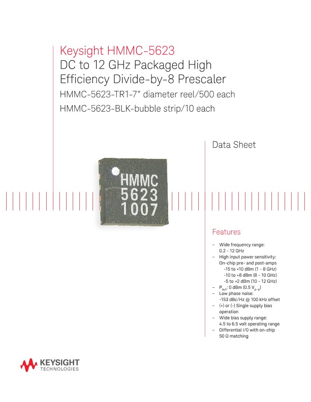
HMMC-5623
DC to 12 GHz Packaged High Efficiency Divide-by-8 Prescaler
HMMC-5623-TR1 (Tape & Reel)
HMMC-5623-BLK (Bulk)
Description
The HMMC-5623 is a packaged prescaler which offers DC to 12 GHz frequency translation for use in communications and EW systems incorporating high frequency PLL oscillator circuits and signal path down conversion applications. It is fabricated using the Keysight Technologies, Inc. InGaP/GaAs HBT MMIC process.
Applications
The HMMC-5623 is designed for use in high frequency communications, microwave instrumentation, and EW radar systems where low phase-noise PLL control circuitry or broad-band frequency translation is required.
Operation
The device is designed to operate when driven with either a single-ended or differential sinusoidal input signal over a 200 MHz to 12 GHz bandwidth. Below 200 MHz the prescaler input is “slew-rate” limited, requiring fast rising and falling edge speeds to properly divide. The device will operate at frequencies down to dc when driven with a square-wave. Due to the presence of an off-chip RF-bypass capacitor inside the package (connected to the VCC contact on the device), and the unique design of the device itself, the component may be biased from either a single positive or single negative supply bias. The backside of the package is not dc connected to any dc bias point on the device. For positive supply operation, VCC pins are nominally biased at any voltage in the +4.5 to +6.5 volt range with pin 8 (VEE) grounded. For negative bias operation VCC pins are typically grounded and a negative voltage between -4.5 to -6.5 volts is applied to pin 8 (VEE).
AC–Coupling and DC-Blocking
All RF ports are dc connected on-chip to the VCC contact through on-chip 50 Ω resistors. Under any bias conditions where VCC is not dc grounded the RF ports should be ac coupled via series capacitors mounted on the PC-board at each RF port. Only under bias conditions where VCC is dc grounded (as is typical for negative bias supply operation) may the RF ports be direct coupled to adjacent circuitry or in some cases, such as level shifting to subsequent stages. In the latter case the package heat sink may be “floated” and bias applied as the difference between VCC and VEE.
Input DC Offset
If an RF signal with sufficient signal to noise ratio is present at the RF input lead, the prescaler will operate and provide a divided output equal the input frequency divided by the divide modulus. Under certain “ideal” conditions where the input is well matched at the right input frequency, the component may “self-oscillate”, especially under small signal input powers or with only noise present at the input This “self-oscillation” will produce an undesired output signal also known as a false trigger. To prevent false triggers or self-oscillation conditions, apply a 20 to 100 mV dc offset voltage between the RFin and RF in ports. This prevents noise or spurious low-level signals from triggering the divider. Adding a 10 kΩ resistor between the unused RF input to a contact point at the VEE potential will result in an offset of ª25 mV between the RF inputs. Note however, that the input sensitivity will be reduced slightly due to the presence of this offset.
Assembly Notes
Independent of the bias applied to the package, the backside of the package should always be connected to both a good RF ground plane and a good thermal heat sinking region on the PC board to optimize performance. For single-ended output operation the unused RF output lead should be terminated into 50 Ω to a contact point at the VCC potential or to RF ground through a dc blocking capacitor. A minimum RF and thermal PC board contact area equal to or greater than 2.67 × 1.65 mm (0.105” × 0.065”) with eight 0.020” diameter plated-wall thermal vias is recommended. MMIC ESD precautions, handling considerations, die attach and bonding methods are critical factors in successful GaAs MMIC performance and reliability. Keysight Technologies GaAs MMIC ESD, Die Attach and Bonding Guidelines - Application Note, literature number 5991-3484EN provides basic information on these subjects. Moisture Sensitivity Classification: Class 5A, per JESD22-A112-A.
RoHS Compliance
This device is RoHS Compliant. This means the component meets the requirements of the European Parliament and the Council of the European Union Restriction of Hazard-ous Substances Directive 2011/65/EU, commonly known as RoHS. The six regulated substances are lead, mercury, cadmium, chromium VI (hexavalent), polybrominated biphenyls (PBB) and polybrominated biphenyl ethers (PBDE). RoHS compliance implies that any residual concentration of these substances is below the RoHS Directive’s maximum concentration values (MVC); being less than 1000 ppm by weight for all substances except for cadmium which is less than 100 ppm by weight.
Oscilloscopes
Analyzers
Meters
Generators, Sources, and Power Supplies
Software
Wireless
Modular Instruments
Network Test and Security
Network Visibility
Services
Additional Products

