Keysight 1GC1-4268
DC - 12 GHz Packaged
Divide-by-2 Prescaler
HMMC-5624-BLK 7” diameter reel/500 each
HMMC-5624-TR1 bubble strip/10 each
Data Sheet
Description
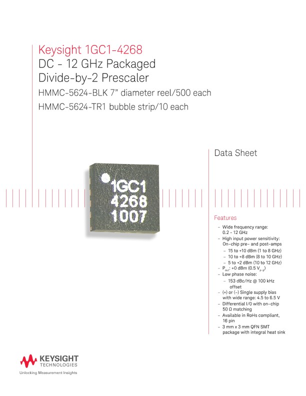
The 1GC1-4268 is a packaged GaAs HBT MMIC prescaler which offers DC to 12 GHz frequency translation for use in communications and EW systems incorporating high– frequency PLL oscillator circuits and signal–path down conversion applications. The differential I/O compatible prescaler provides a large input power sensitivity window, low phase noise and is packaged in a 3 mm x 3 mm 16-pin QFN SMT package.
Applications
The 1GC1-4268 is designed for use in high frequency communications, microwave instrumentation, and EW radar systems where low phase–noise PLL control circuitry or broadband frequency translation is required.
Operation
The device is designed to operate when driven with either a single–ended or differential sinusoidal input signal over a 200 MHz to 12 GHz bandwidth. Below 200 MHz the prescaler input is “slew–rate” limited, requiring fast rising and falling edge speeds to properly divide. The device will operate at frequencies down to DC when driven with a square–wave. Due to the presence of an off–chip RF–bypass capacitor inside the package (connected to the Vthe device), and the unique design of the device itself, the component may be biased from either a single positive or single negative supply bias. The backside of the package is not directly connected to any DC bias point on the device. For positive supply operation, VCC pins are nominally biased at any voltage in the +4.5 to +6.5 volt range with pin 8 (V EE ) grounded. For negative bias operation VCC pins are typically grounded and a negative voltage between -4.5 to -6.5 volts is applied to pin 8 (VEE).
AC–coupling
All RF ports are DC connected on–chip to the VCC contact through on– chip 50 Ω resistors. Under any bias conditions where VCC is not DC grounded, the RF ports should be AC coupled via series capacitors mount- ed on the PC–board. Only under bias conditions where VCC is DC grounded (as is typical for negative bias supply operation) may the RF ports be direct coupled to adjacent circuitry or in some cases, such as level shifting to subsequent stages. In the latter case the package heat sink may be “floated” and bias applied as the difference between VCC and VEE.
Input DC offset
If an RF signal with sufficient signal to noise ratio is present at the RF input pin, the prescaler will operate and provide a divided output equal the input frequency divided by the divide modulus. Under certain “ideal” conditions where the input is well matched at the right input frequency, the component may “self–oscillate”, especially under small signal input powers or with only noise present at the input. This “self–oscillation” will produce a undesired output signal also known as a false trigger. To prevent false triggers or self–oscillation conditions, apply a 20 to 100 mV DC offset voltage between the RFin and RFin ports. This prevents in innoise or spurious low level signals from triggering the divider. Adding a 10 KΩ resistor between the unused RF input to a contact point at the VEE potential will result in an offset of 25 mV between the RF inputs. Note however, that the input sensitivity will be reduced slightly due to the presence of this offset. An input DISABLE pin is also provided to allow the prescaler input pre-amp to be locked into either a logic “High” or “Low” state, thereby preventing false triggers.
Assembly Techniques
Independent of the bias applied to the package, the backside of the package should always be connected to both a good RF ground plane and a good thermal heat sinking region on the PC–board to optimize performance. For single–ended output operation, the unused RF output pin should be terminated into 50 Ω to a contact point at the VCC potential or to RF ground through a DC blocking capacitor. Figure 2 shows the package / PCB assembly diagram for single–ended or differential input frequency operation through 12 GHz. For positive supply operation, VCC is typically biased to a positive voltage between +4.5 and +6.5 volts and VEE is grounded. For negative supply operation, VEE is typically biased between –4.5 to –6.5 volts and VCC is grounded. In either case, the supply contact to the package bias pin(s) must be capacitively bypassed (0.01 mF, recommended) to provide good bias stability, input sensitivity and low input power feed through. The bypass capacitor should be located as close as possible to the package pin. In general, AC coupling capacitors are recommended on the RFin and RFout connections to the package. For positive supply operation, VCC is positively biased resulting in a positive DC voltage appearing at RFin or RFout. In this case a AC coupling cap is required. For singulated package dimensions of the 3 mm x 3 mm QFN package, refer to Figure 3. The QFN SMT package is compatible with industry standard solder-reflow attach processes.
Oscilloscopes
Analyzers
Meters
Generators, Sources, and Power Supplies
Software
Wireless
Modular Instruments
Network Test and Security
Network Visibility
Services
Additional Products

