What are you looking for?
Device Modeling and Characterization
Turnkey solutions for device modeling and characterizing CMOS, RF, and III-V devices
From integrated device manufacturers (IDMs) to top foundries, Keysight provides trusted one-stop solutions that measure, extract, and validate the world’s semiconductor devices. With over two decades of expertise, Keysight's end-to-end device modeling and device characterization solutions, coupled with expert support and state-of-the-art labs, have empowered hundreds of customers to accurately and efficiently model CMOS, RF, and wide-bandgap semiconductor devices.
Device Modeling and Device Characterization Solutions
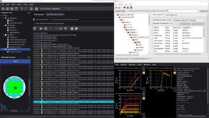
- PathWave Device Modeling (IC-CAP)is versatile, user-programmable industry standard software for DC, analog, and RF semiconductor device characterization and modeling. Today's most advanced semiconductor foundries and IDMs rely on IC-CAP for modeling silicon CMOS, bipolar, compound gallium arsenide (GaAs), gallium nitride (GaN), and many other device technologies.
- PathWave Model Builder (MBP) provides complete silicon turnkey device modeling software that integrates SPICE modeling and simulation, model parameter extraction, and model library generation.
- PathWave Model QA (MQA)is the industry-standard SPICE model validation software, enabling thorough check-model quality and automatic QA and reporting procedures for both silicon and III-V technologies.
- PathWave WaferPro (WaferPro Express) supports on-wafer measurement and programming test software for use with a variety of instruments and wafer probes.
- Advanced Low-Frequency Noise Analyzer (A-LFNA) supports on-wafer measurement and analysis of low-frequency noise including flicker noise and random telegraph noise.

Samsung Foundry Adopts Keysight Radio Frequency Device Model Generator
In June, 2023, Keysight announced that Samsung Foundry adopted the new Keysight IC-CAP Model Generator (MG) to accelerate the creation of circuit libraries, a key component of process design kits (PDKs) for Samsung's advanced radio frequency (RF) semiconductor process technologies.
Jongwook Kye, Executive Vice President and Head of Foundry Design Platform Development at Samsung Electronics, said: "Over the past few years, we have been collaborating closely with Keysight EDA to improve the efficiency and accuracy of our RF modeling flow. By adopting the Model Generator in our workflow, our efficiency has improved by at least 30 percent."
How to Extract the ASM-HEMT Model for GaN RF Devices Including Thermal Effects
Gallium Nitride (GaN) high electron mobility transistors (HEMTs) are gaining rapid adoption in high-power, high-voltage, and high-frequency applications due to their superior performance such as high saturation velocity, high breakdown voltage, and high sheet carrier density. However, integrating GaN devices into a circuit design requires accurate and robust circuit simulations. The accuracy of simulations depends on the compact model's ability to predict highly non-linear behavior, including thermal and dynamic memory effects.
Download this application note for a comprehensive extraction procedure for the industry-standard ASM-HEMT model for GaN devices, including self-heating.


Protect Your Innovation Investment


Featured Resources


FREQUENTLY ASKED QUESTIONS
What does device modeling mean in semiconductor design?
Device modeling refers to the process of creating mathematical and physical models to predict the behavior of semiconductor devices, such as transistors, diodes, and capacitors. These models help electronic designers understand how these components perform in various real-world applications.
Why is device modeling important in semiconductor and electronic designs?
Device modeling allows design engineers to optimize their designs for specific requirements, such as maximizing speed or minimizing power consumption. By simulating device behavior under different conditions, engineers can effectively reduce the need for expensive physical prototypes, thereby saving time and resources.
What is a typical flow of device modeling and device characterization?
The typical flow of device modeling and characterization consists of four critical steps, with each integral to the quality and reliability of the final models:
- Data measurement and analysis: This first stage involves gathering measured data from various semiconductor devices across different wafers and temperatures. The focus here is on precision and efficiency.
- Model extraction: Model extraction complexity varies with the technology and specific device model. Device modeling software is instrumental at this stage, offering advanced graphics, links to circuit simulators, optimizers, and manual tuners to extract parameters. For RF modeling, custom programming might be necessary to account for parasitic effects in S-parameters.
- Model validation: This step is fundamental to ensure the reliability of the modeling libraries by running simulations over extended bias, geometry, and frequency conditions. Tools like MQA (Model Quality Assurance) can automate much of this process, simplifying the testing and helping to identify and report any issues efficiently.
- Integration into process design kits (PDKs): The final step involves integrating device modeling libraries into PDKs. A critical but challenging aspect of this phase is PDK validation, which involves extensive re-verification of sample designs whenever there's a new release of a simulator software version or an update to a design kit. The goal is to ensure that the PDKs remain accurate and consistent across different updates.
Want help or have questions?